|
|
| Designing with the IMS T414 and IMS T800 memory interface _____________________________________________________________________ |
| Tony Gore and David Cormie August 1987 |
The configurable memory interface of the T414 transputer greatly simplifies memory system design, making it easier to implement systems with little or no previous experience.
This document describes the use of the external memory interface of the T414 transputer to interface a variety of memory types.
The T800 has the same memory interface as the T414, so for ”T414” read ”T414 and T800”.
The T414 has a configurable memory interface designed to allow easy interfacing of a variety of external memory types with minimal extra components. The T414 interface can directly support DRAMs, SRAMs, ROMs and memory mapped peripherals.
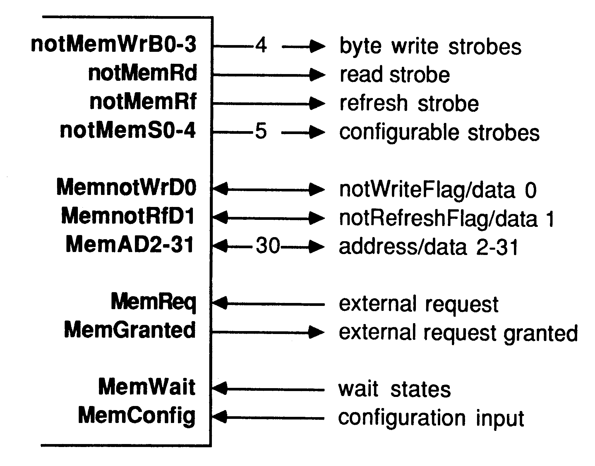
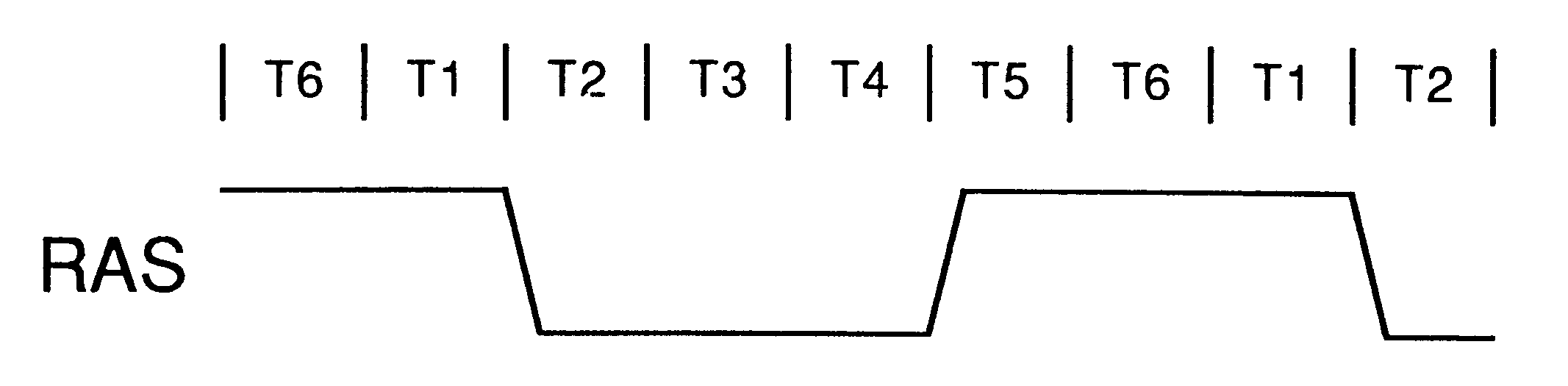
The T414 has a 32 bit multiplexed data and address bus with a linear address space of 4 Gbytes. There are 4 byte write strobes, a read strobe, a refresh strobe, 5 configurable strobes, a wait input, a memory configuration input, a bus request input and bus grant output. Figure 1 shows the inputs and outputs for the T414 transputer that are associated with the memory interface.
With this flexible arrangement, a variety of memory timing controls can be obtained with little external hardware. An example of bus timing is shown in figure 2.
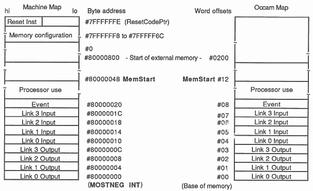
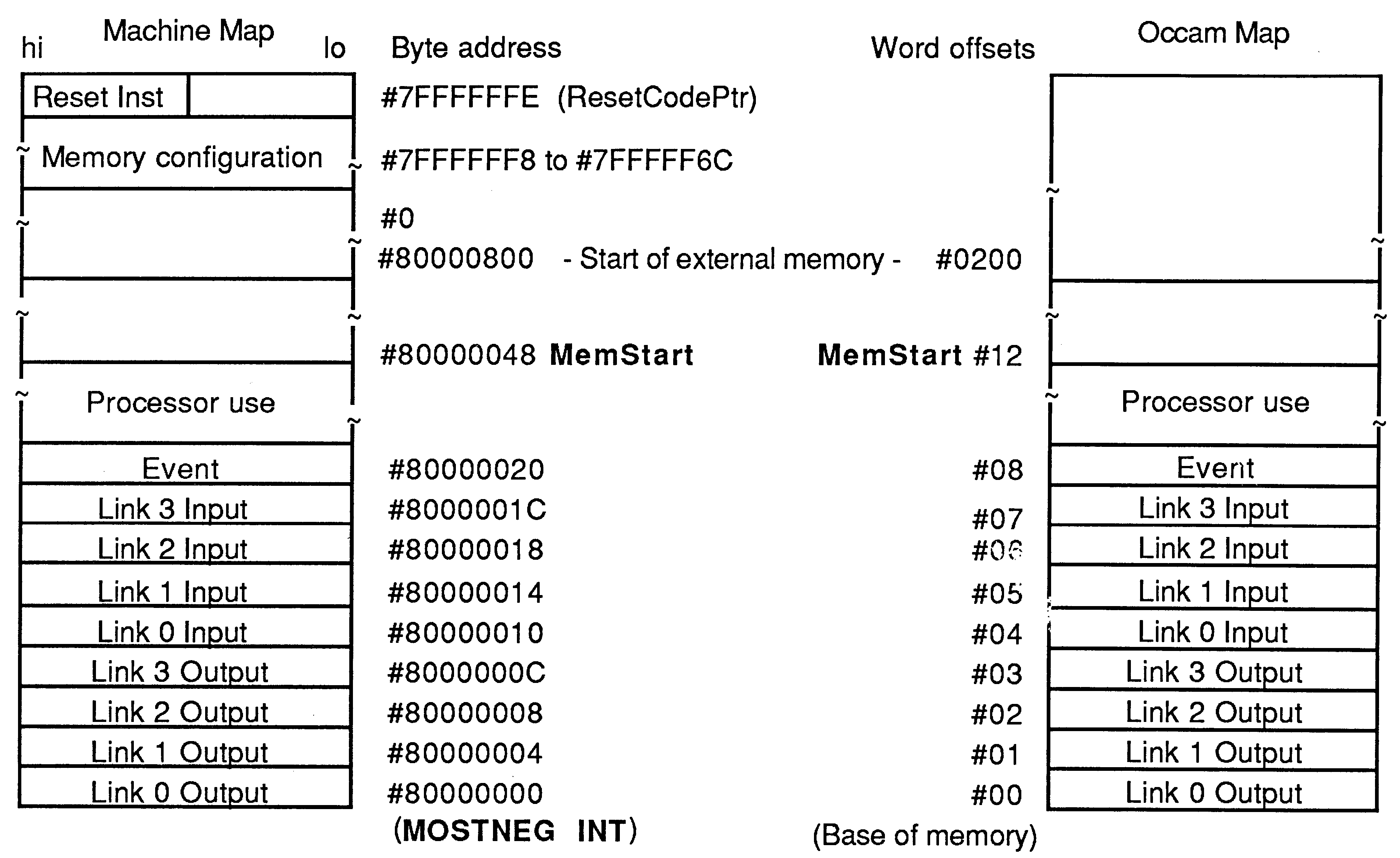
The T414 has a signed address space and addresses memory as bytes. Addresses, therefore, run from $80000000 through $FFFFFFFF to $7FFFFFFF. This differs from the occam map which starts at $0 and is organised as words. Thus MemStart is at $80000048 in the machine map and $12 in the occam map. The comparison is given in figure 3.
Throughout this application note, all addresses referred to will be those for the machine map.
The T414 has 2Kbytes of on-chip RAM at addresses $80000000 to $800007FF. It is, therefore, advisable for $80000000 to $FFFFFFFF to be used for RAM and $00000000 to $7FFFFFFF to be used for ROM and I/O. If internal memory and external memory exist at the same address, the transputer will access internal memory. Note that if the memory map is not completely decoded, it is usually possible to access the ”hidden” external memory at another address; e.g. on the B004-2, the hidden memory can actually be accessed at $80200000 to $802007FF.
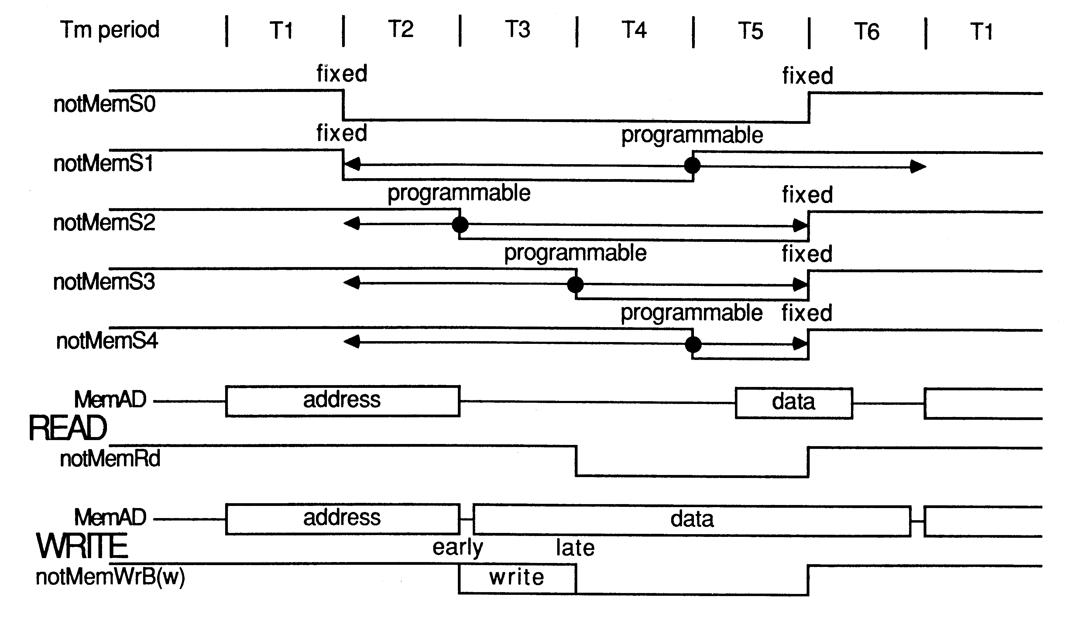
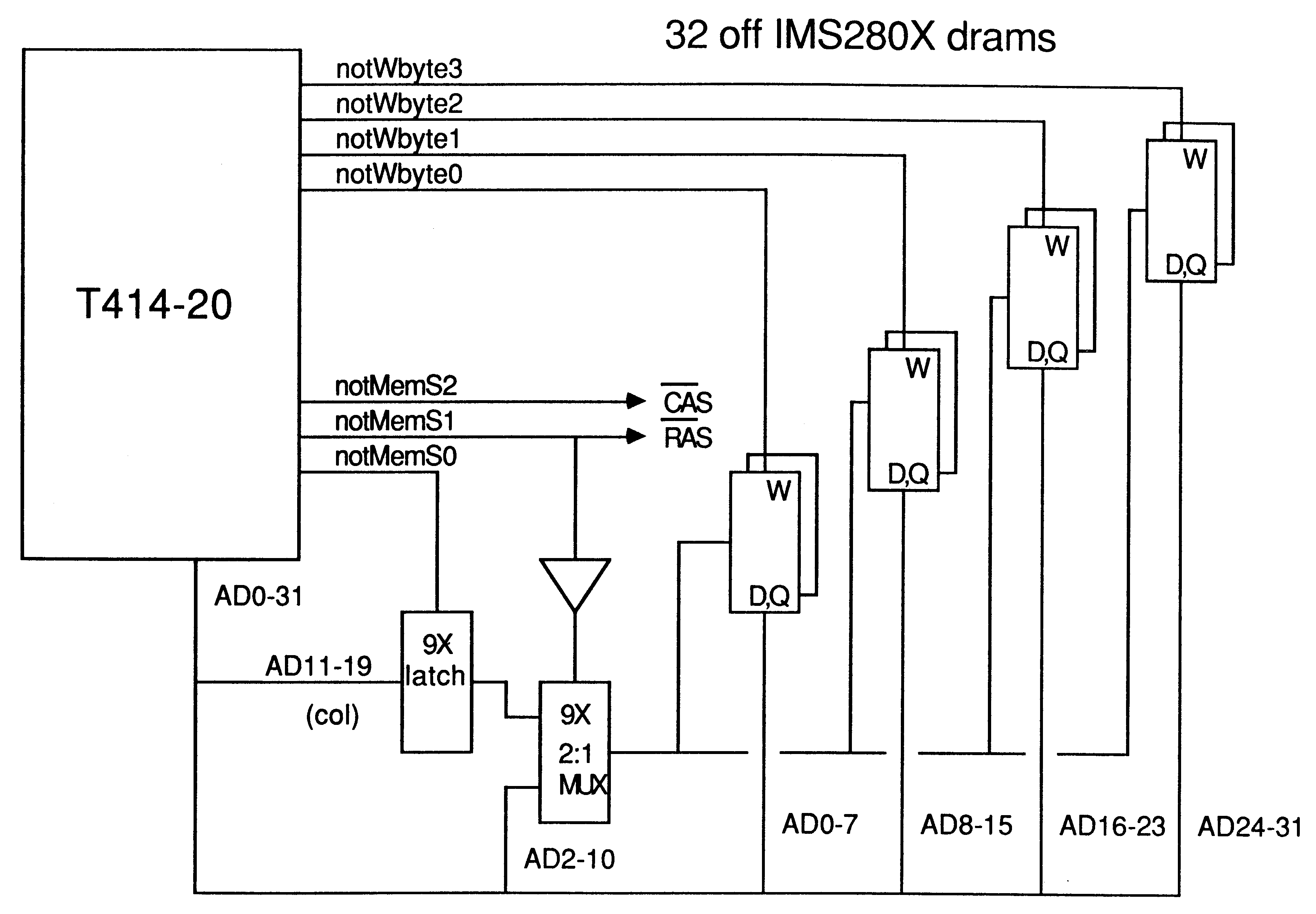
The T414 memory interface cycle has six timing states, referred to as Tstates. The Tstates have the nominal functions:
| Tstate | |
| T1 | address setup time before address valid strobe |
| T2 | address hold time after address valid strobe |
| T3 | read cycle tristate/write cycle data setup |
| T4 | extended for wait states |
| T5 | read or write data |
| T6 | end tristate/data hold |
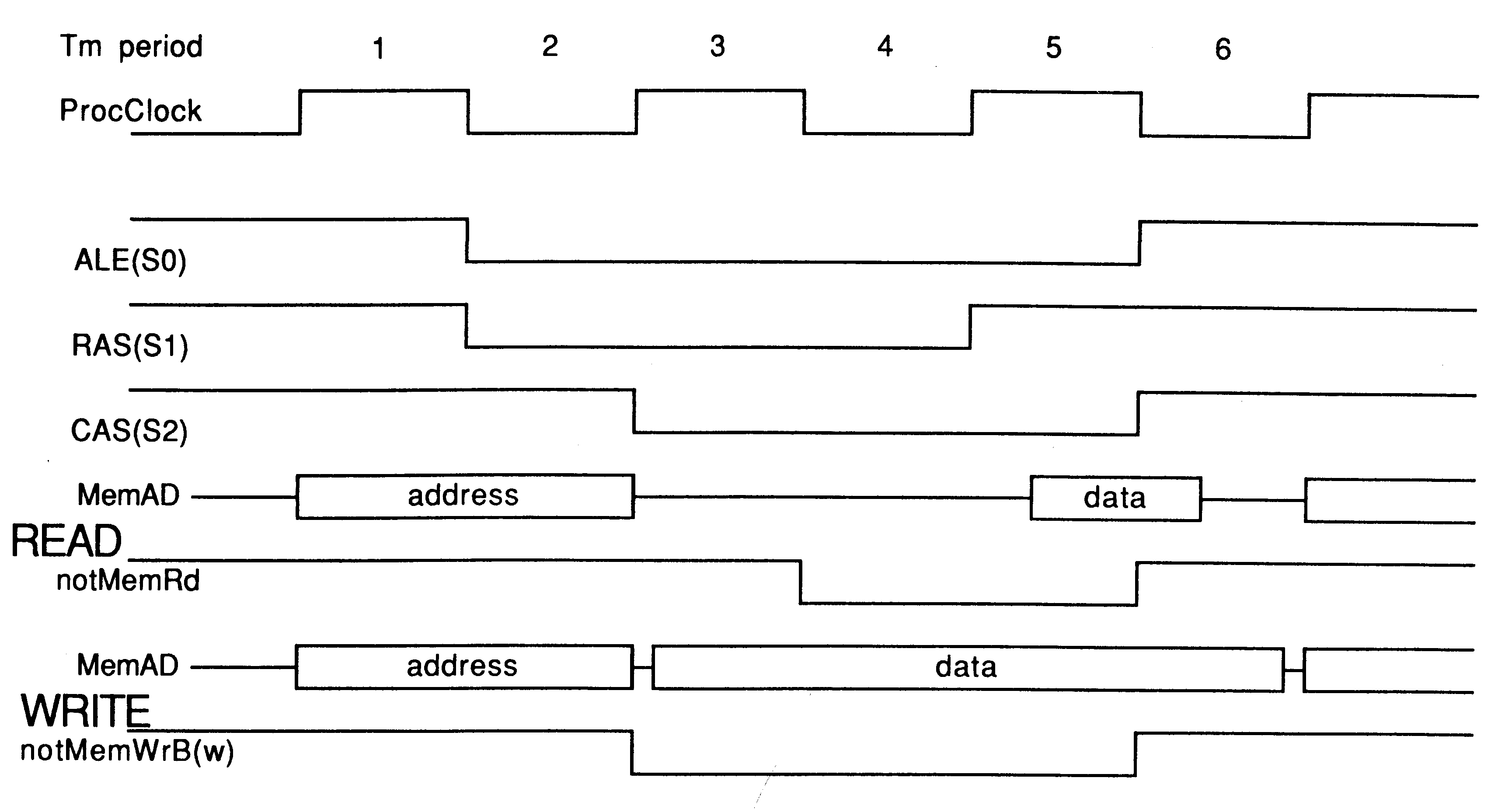
The duration of each Tstate is configurable to suit the memory devices used and can be from one to four Tm periods. One Tm period is half the processor cycle time; i.e. half the period of ProcClockOut. Thus, Tm is 25nsec for a T414-20 (20MHz transputer). T4 may be extended by wait states in the form of additional Tms. A0 and A1 are not output with the rest of the address. During a write cycle, byte and half-word (16 bit data) addressing is achieved by the four write byte strobes (notMemWrB): only the write strobes corresponding to the bytes to be written are active. During a read cycle, this is achieved by internally selecting the bytes to be read.
Thus, the two lowest order address lines are not needed. However, care must be taken when mapping byte wide peripherals onto the interface, as they will have to be addressed on word boundaries.
The two lowest order data lines are not multiplexed with address lines but, during the address period, are used to give early indication of the type of cycle which will follow:
MemnotWrD0 is low during T1 and T2 of a write cycle.
MemnotRfD1 is low during T1 and T2 of a refresh cycle.
The use of the strobes notMemS0 to notMemS4 will depend upon the memory system. The rising edge of notMemS1 and the falling edges of notMemS2 to notMemS4 can be configured to occur from 1 to 31 Tm periods after the start of T2. This is summarised in figure 2 and in the table below.
| Signal | Starts | Ends |
| notMemS0 | T2 | T6 |
| notMemS1 | T2 | T2 + (Tm*s1) (or end of T6 if this occurs first) |
| notMemS2 | T2 + (Tm*s2) | T6 |
| notMemS3 | T2 + (Tm*s3) | T6 |
| notMemS4 | T2 + (Tm*s4) | T6 |
It should be noted that the use of wait states can advance the rising edge of notMemS1 in relation to that of the other strobes; care must be taken if this signal is being used for RAS driving DRAMs for which RAS must not be removed before CAS; this is not a problem with the new generation Inmos IMS2800/1/2/3/4 256k DRAMs.
The notMemWrB strobes can be configured to fall either at the beginning of T3 (early write) or at the beginning of T4 (late write); the rising edge is always at the beginning of T6. Early write gives a longer set up time for the write strobe but data is only valid on the rising edge of the pulse. For late write, data is also valid on the falling edge of the strobe but the pulse is shorter.
The T414 has an on-chip refresh controller and 10 bit refresh address counter and can, therefore, refresh DRAMs of up to 1 Mbit by 1 capacity without requiring the counter to be extended externally.
Refresh can be configured to be either enabled or disabled. If enabled, the refresh interval can be configured to be 18, 36, 54 or 72 Clockln periods; though if a refresh cycle is due, the current memory cycle is always completed first. The time between refresh cycles is thus almost independant of transputer speed and the length of memory cycles.
Refresh cycles are flagged by notMemRf going low before T1 and remaining low until the end of T6. Refresh is also indicated by MemnotRfD1 going low during T1 and T2 with the same timing as address signals. The address output during refresh is:
| AD0 | = MemnotWrD0 | high |
| AD1 | = MemnotRfD1 | low, to indicate refresh |
| AD2 - AD11 | refresh address | |
| AD12 - AD30 | high | |
| AD31 | low | |
During refresh cycles, the strobes notMemS0 - notMemS4 are generated as normal.
Memory cycles can be extended by wait states. MemWait is sampled close to the falling edge of ProcClockOut prior to, but not at, the end of T4. If it is high, T4 is extended by additional Tms (shown as ”W” by the memory interface program). Wait states are inserted for as long as MemWait is held high, T5 proceeds when MemWait is low. Note that the internal logic of the memory interface ensures that, if wait states are inserted, T5 always begins on a rising edge of ProcClockOut: so the number of wait states inserted will be either always odd or always even, depending on the memory configuration being used.
Every memory interface cycle must consist of a number of complete cycles of ProcClockOut: i.e. it must consist of an even number of Tms. If there are an odd number of Tm periods up to and including T6, an extra Tm (shown as ”E” by the memory interface program) will be inserted after T6.
A memory interface configuration is specified by a 36 bit word and is fixed at reset time. The T414 has a selection of 13 pre-programmed configurations. If none of these is suitable, a different configuration can be selected by supplying the complement of the configuration word to the T414s MemConfig input immediately following reset.
A pre-programmed configuration is selected by connecting MemConfig to MemnotWrD0, MemnotRfD1, MemAD2-MemAD11 or MemAD31. Immediately after reset, the T414 takes all of the data lines high and then, beginning with MemnotWrD0, they are taken low in sequence. If MemConfig goes low when the T414 pulls a particular data line low, the memory interface configuration associated with that data line is used. If, during the scan, MemConfig is held low until MemnotWrD0 goes low, or is connected to MemAD31, the slowest memory configuration is used.
After scanning the data lines as described above, the T414 performs 36 read cycles from locations $7FFFFF6C, $7FFFFF70 - $7FFFFFF8. No data is latched off the data bus but, if MemConfig was held low until MemnotWrD0 was taken low, each read cycle latches one bit of the (inverted) configuration word on MemConfig. Thus, a memory configuration can be supplied by external logic.
Using a pre-programmed configuration has the advantage of requiring no external components: only a connection from MemConfig to the appropriate data line. However, selecting an external configuration can also be very economical in component use. If the transputer is booting from ROM, the ROM must occupy the top of the address space. One bit of the memory configuration word can be stored in each of the 36 addresses mentioned above and the only additional hardware required is an inverter connecting the appropriate data line (usually MemnotWrD0) to MemConfig. MemConfig is thus held low until MemnotWrD0 goes low and is fed with the inverse of the configuration word during the 36 read cycles. Alternatively, the inverted configuration word can be generated from A2-A7 by one product term of a PAL.
The INMOS Transputer Development System includes an interactive program which assists in the task of memory interface design. The program produces timing diagrams and timing information so that the designer can see the effects of varying the length of each Tstate and the positions of the programmable strobe edges. Of course, the program cannot allow for external logic delays and loading effects as these are system dependant but it does assist greatly in preliminary design.
The minimum number of processor clock cycles for an external memory access is 3, which occurs when all Tstates are 1 Tm. With a 50 nsec cycle time, this will be 150 nsec.
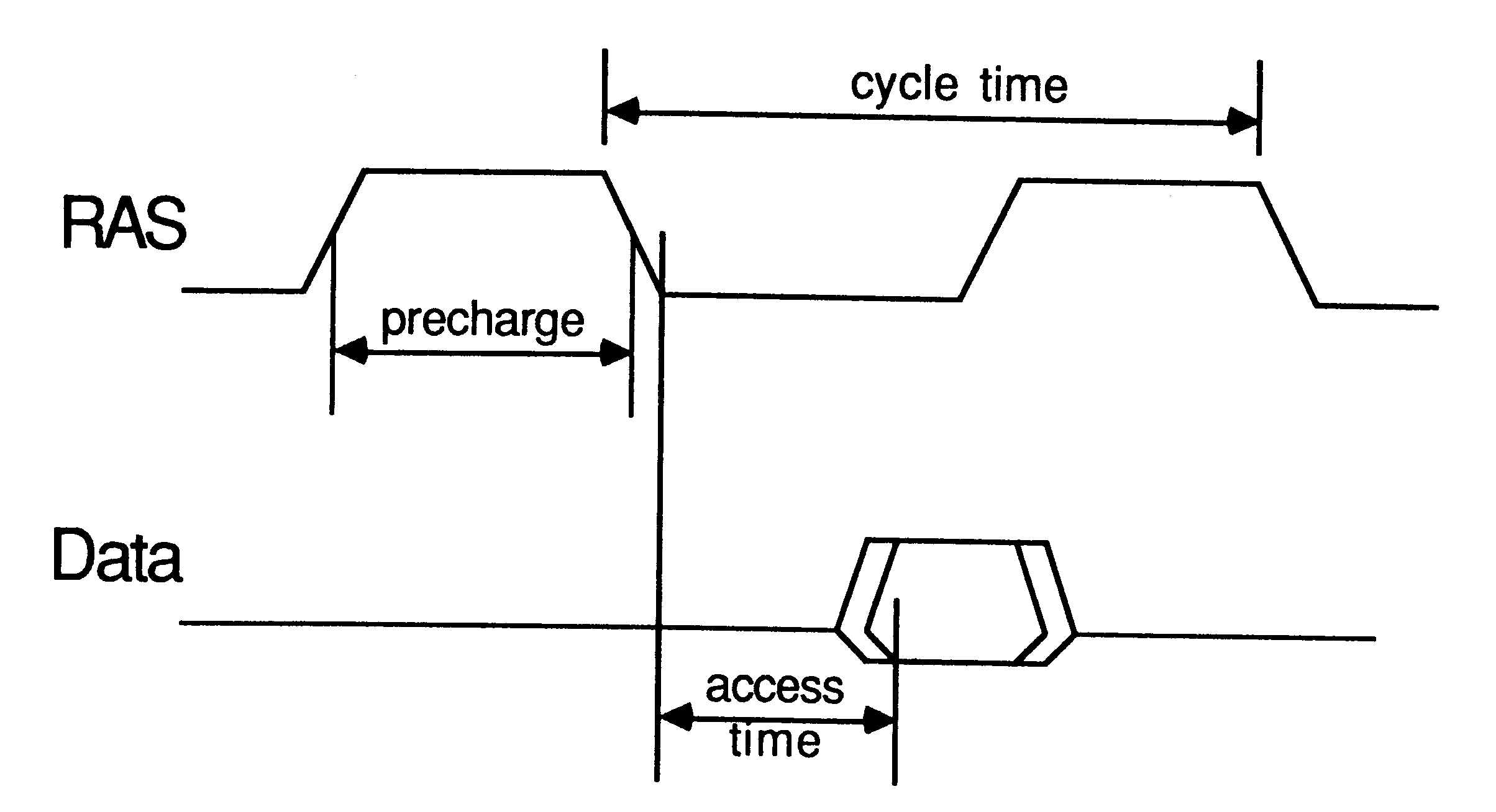
The most important DRAM parameters to be considered at the start of a memory design are the access and cycle times and the RAS precharge time. These will be a guide to the fastest timing possible, which is generally a good starting point, and are defined in figure 4.
Parameters for typical Dynamic RAMS:
| NEC | uPD41256-15 | ||
| Access time | 150ns | ||
| Cycle time | 270ns | ||
| RAS precharge | 100ns | ||
| Inmos | IMS2800-150 | IMS2800-80 | IMS2800-60 |
| Access time | 150ns | 80ns | 60ns |
| Cycle time | 246ns | 151ns | 121ns |
| RAS precharge | 90ns | 65ns | 55ns |
Higher density devices require longer RAS precharge times but, if the memory does not require RAS to remain low until the end of the memory cycle, it can be taken high before the cycle ends, thus easing the designer’s job of finding adequate precharge time whilst minimising the amount of time to be added to the DRAM cycle time.
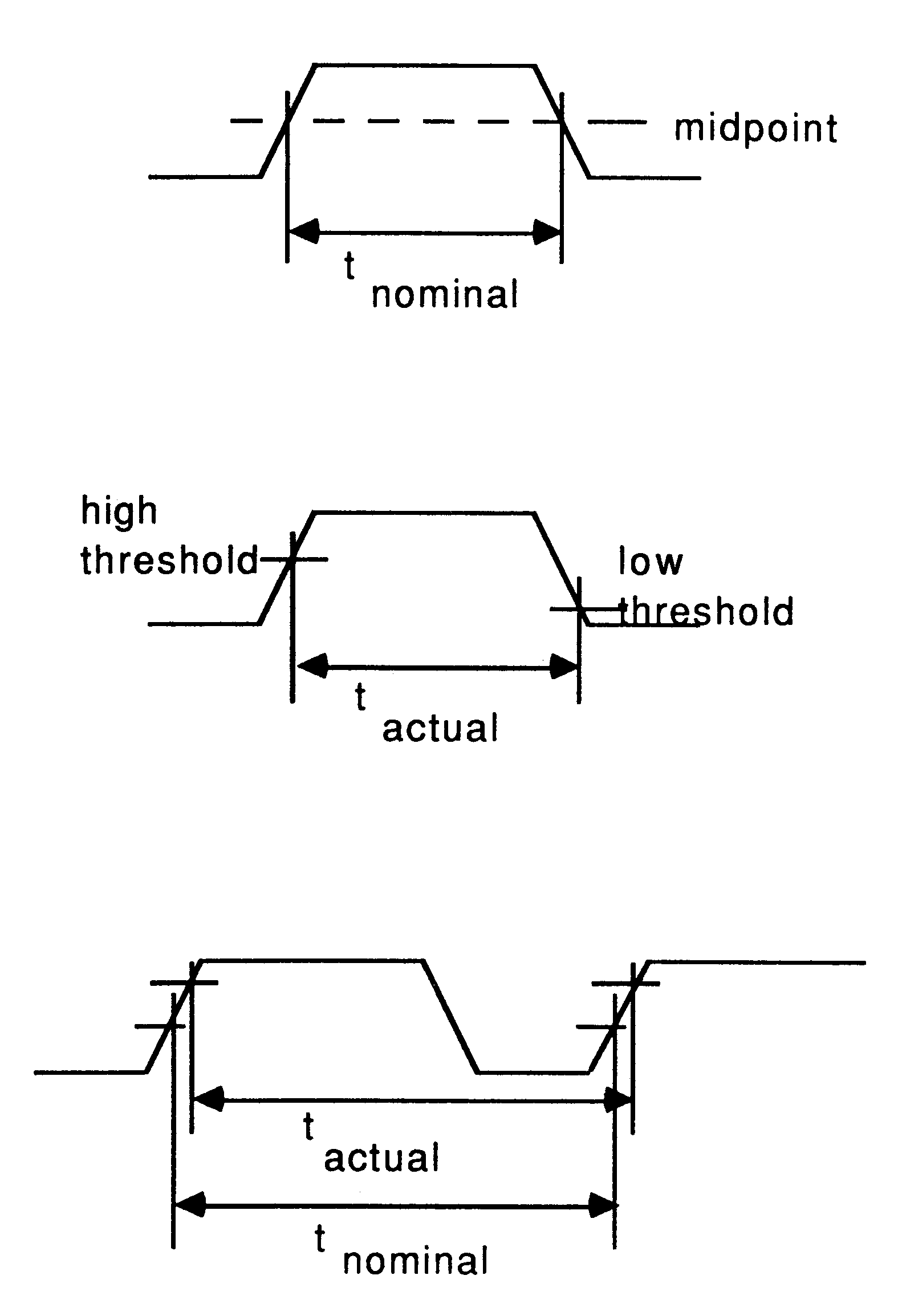
When calculating memory interface timings, consideration must be given to propagation delay and skew through buffers and decoding. Skew occurs where there are different logic thresholds and hence different propagation delays for high going and low going signals. This is shown in figure 5.
It is also important to bear in mind the asymmetric drive capabilities of most logic that would be used externally.
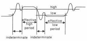
Ringing (figure 6) becomes a problem when signals are called upon to drive a large capacitive load, such as a DRAM array. The high currents required to charge the capacitance have to flow through wiring or PCB tracks, all of which have some inductance, thus creating a tuned circuit. Ideally, the waveform presented will be as steep as possible for minimum propagation delays; however, this implies a large spread of frequencies, including the resonant frequency of the tuned circuit. An alternative way to view the problem is that of driving a transmission line. The solution is to include a series resistor to dissipate the energy in the tuned circuit whilst matching the driver more closely to the transmission line characteristic impedance. The aim is critical damping of the response to the step input. Some DRAM buffers/drivers have the series resistor, or something equivalent, incorporated. e.g. AMD Am2965/6.
This example describes the design of a system based on a T414-20 with:
Warning: A number of common pitfalls exist in this application, and are revealed step by step. Thus the partial circuits should not be used until this complete section has been read and digested.
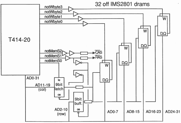
The most compact way to implement the 2 Mbyte memory is as two banks of 256kx1 bit DRAMs. This requires 64 devices.
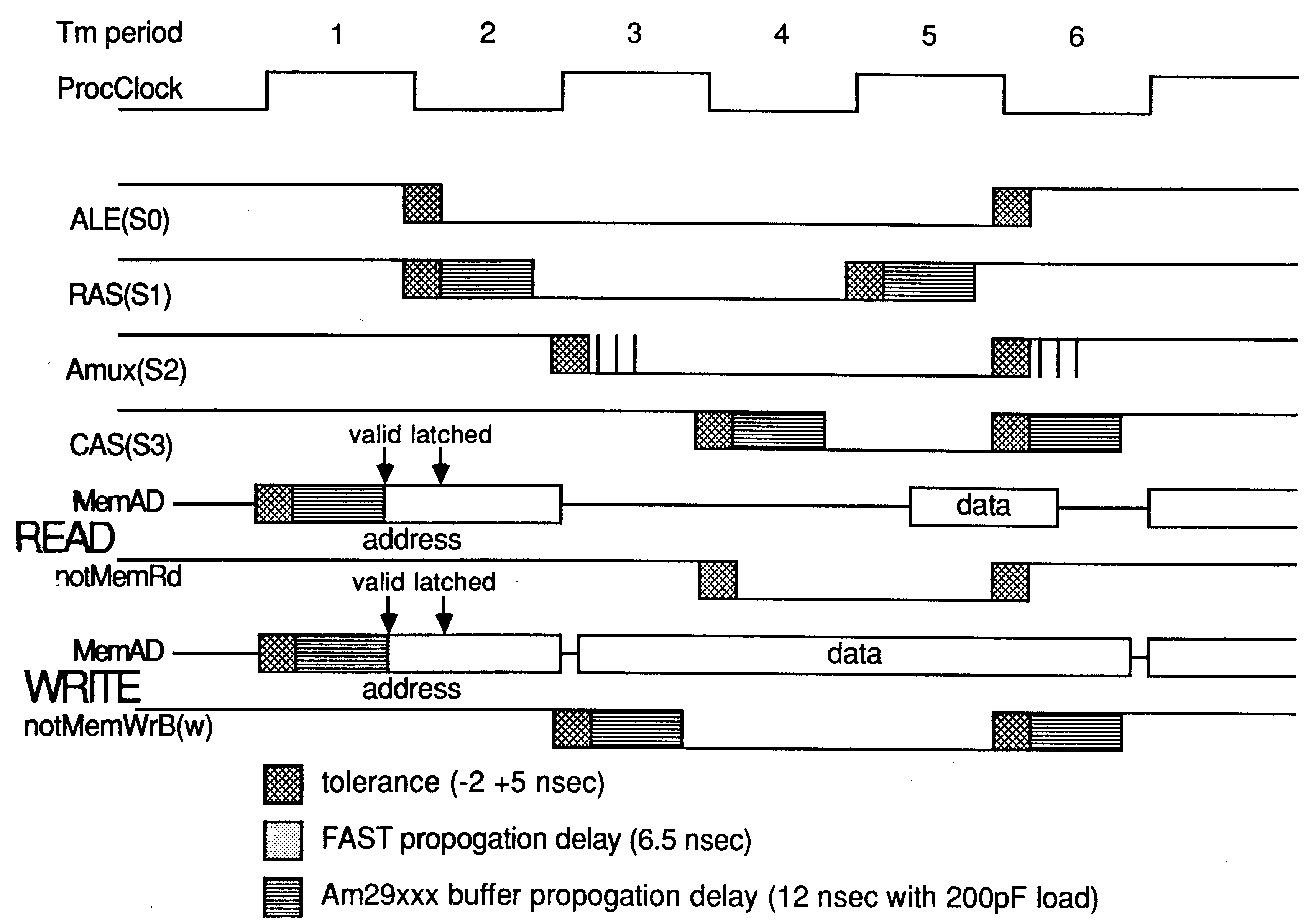
A T414-20 has been specified as the design goal. This gives a Tm period of 25 nsec. To run as fast as possible, let T1-T6 each be 1 Tm in length; giving an external memory cycle time of 150 nsec. Such a short memory cycle time requires the use of a fast, high performance DRAM such as one of the IMS280x series: IMS2800, 2801, 2802, 2803 & 2804.
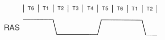
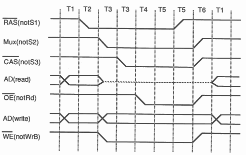
With only 3 processor cycles, there is only one realistic possibility, as shown in figure 7, namely RAS low for three Tm periods. RAS low for two Tm periods would require a 50 nsec access DRAM and RAS low for four Tm periods leaves only 50 nsec for RAS precharge. Neither of these is possible with current DRAMs.
Most current EPROMs and peripherals cannot run at a cycle time of 150 nsec. The fastest widely available EPROMs are 150nsec access. Thus it will be necessary to insert wait states when EPROMs and peripherals are accessed. To maximise the system performance it will be necessary to have two different lengths of wait states, one for ROM and one for peripherals, requiring the use of two of the transputer’s programmable strobes. This means that only a change to the memory configuration will be required at a later date to upgrade to faster parts. Therefore, we will reserve notMemS3 and notMemS4 as two separate wait state generators, since the point at which they go low is the feature that is user programmable.
This leaves 3 strobes, notMemS0-2 for total DRAM control.
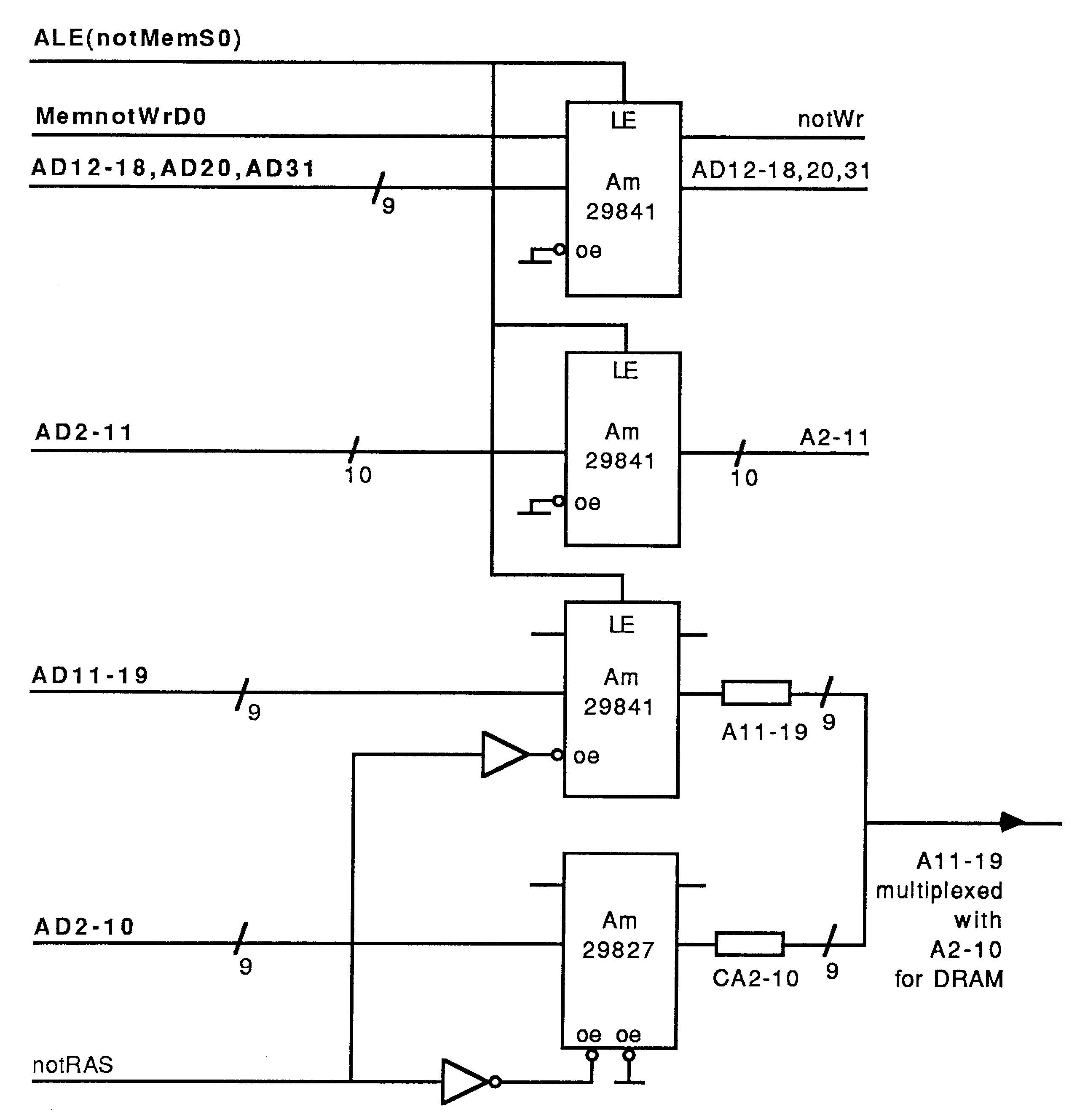
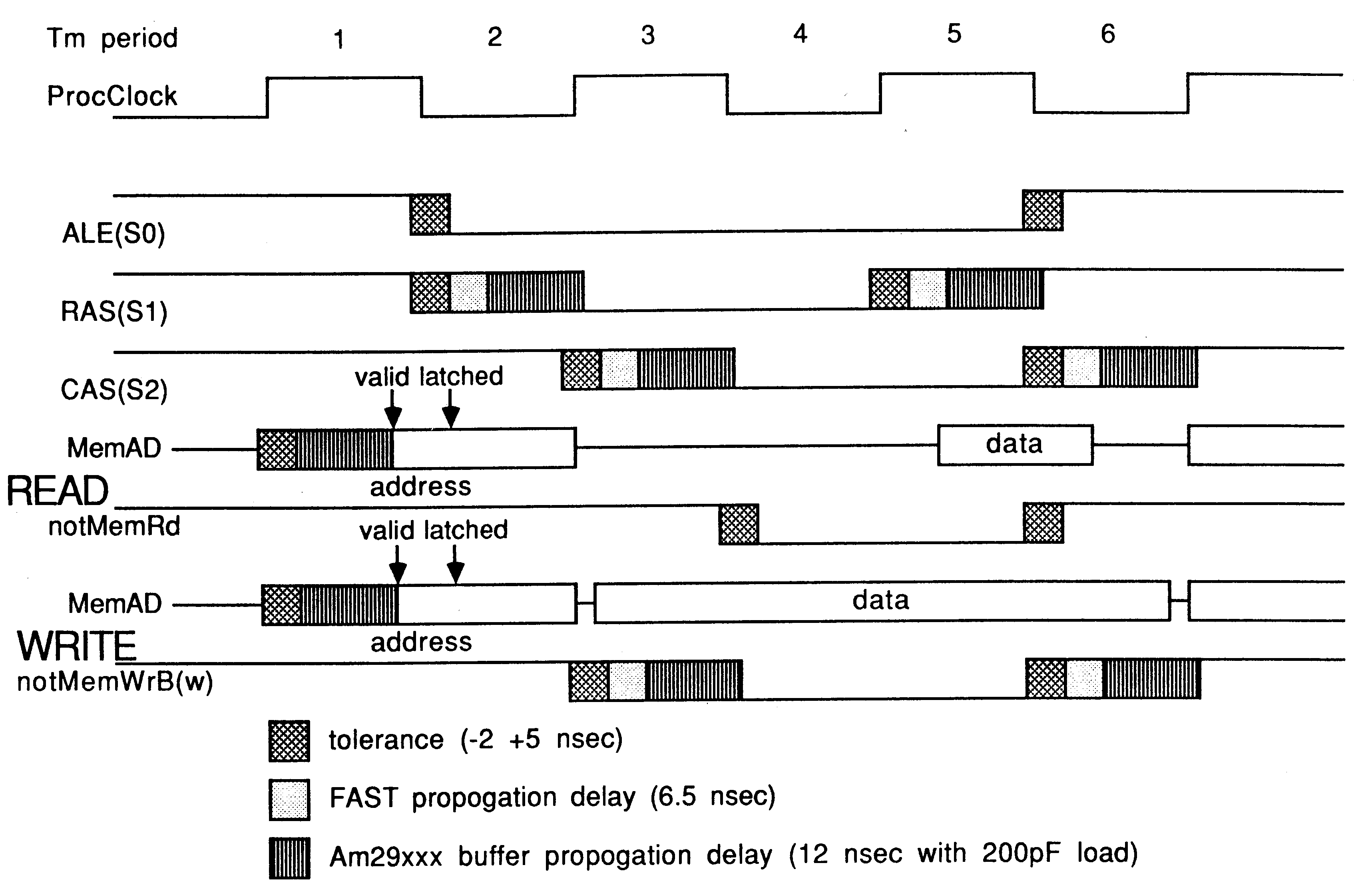
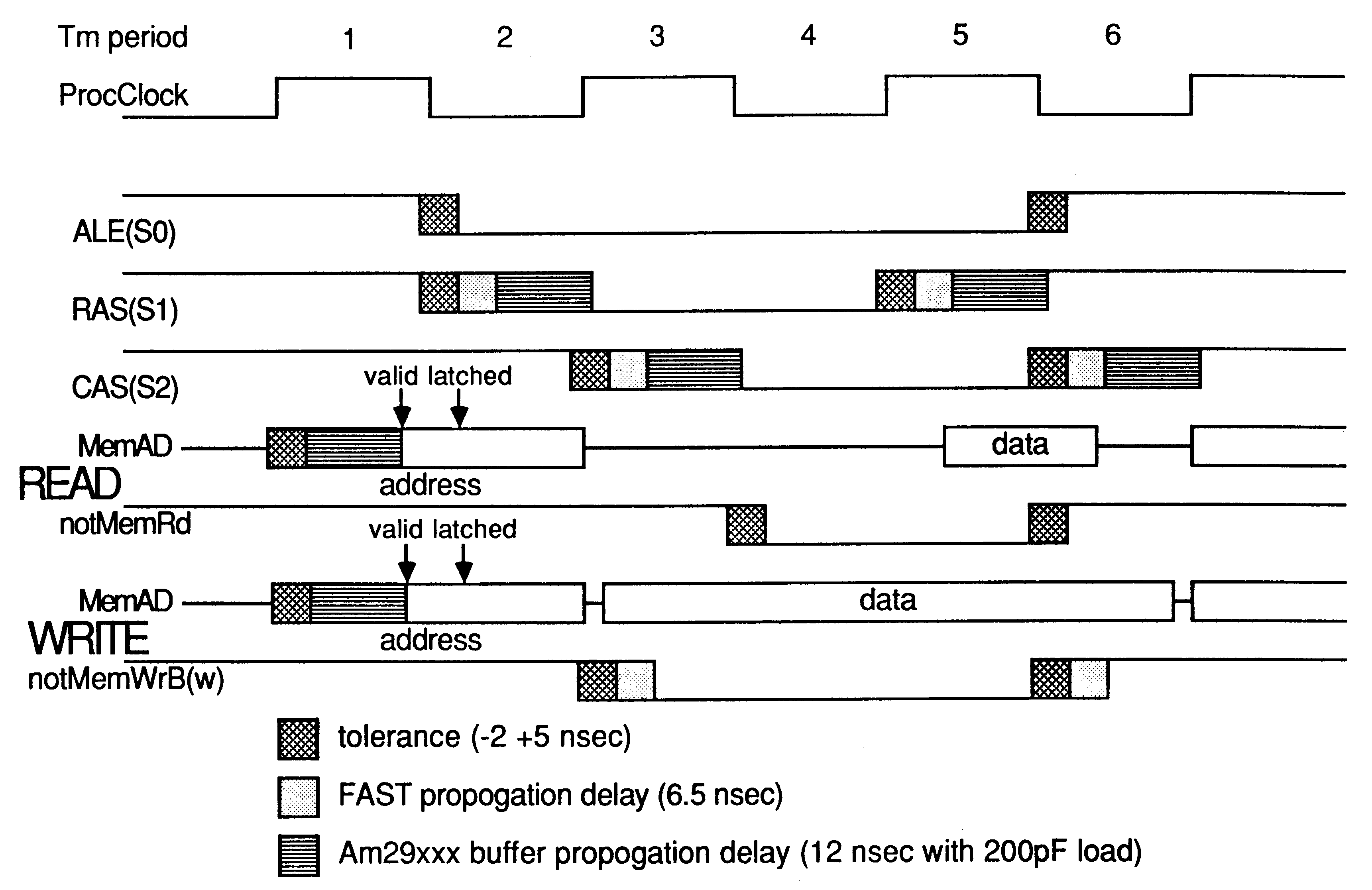
notMemS0 goes low at the start of T2 and high at the start of T6, being low for 4 Tm periods in this example, and thus cannot be used for RAS. The data and address lines from the transputer are multiplexed, addresses being valid for T1 and T2, so notMemS0 can be used to latch the address.
notMemS1 goes low at the start of T2 and the duration of its low period is programmable. It can, therefore, be used as RAS because RAS must go low at the beginning of T2 and high at the beginning of T5 to meet the precharge time.
notMemS2 has a programmable falling edge and goes high at the beginning of T6. It can, therefore, be used as CAS. To allow sufficient data set up time during read cycles, and sufficient CAS/RAS lead time, notMemS2 must fall at the beginning of T3.
We require one further signal, usually called Amux, which is used to switch between the row and column addresses supplied to the DRAM. Normally, as in the simple example, notMemS2 would be used for this and notMemS3 for CAS, leaving notMemS4 for wait state generation but, in this case, we can make use of one of the features of the IMS280x series DRAMs: that of short row address hold time (tRL1AX), which is only 2 nsec. This allows the RAS strobe delayed by 2nsec or more to be used as Amux.
The preliminary circuit and timing are shown in figures 8 and 9.
The RAM must occupy the bottom of the address space so that it appears to be a continuation of the transputer’s internal RAM. The ROM must occupy the top of the address space, so that the transputer can boot from ROM. We can, therefore, use A31 to select between RAM and ROM. A2-A19 will be used to address the DRAMs so we should use A20 to select between banks. We can also use A20 to select between ROM and I/O. This gives a very simple decoding scheme:
| A31 | A20 | |
| 1 | 0 | RAM bank 0 |
| 1 | 1 | RAM bank 1 |
| 0 | 0 | I/O space |
| 0 | 1 | ROM |
For the IMS280x series of DRAMs: any RAS sequence will refresh an entire row of 1024 bits, reading or writing of data is initiated by CAS. Therefore, address decoding need only be applied to CAS; RAS can be enabled to both banks of RAM at all times. Thus, reading or writing one RAM bank will cause the other to be refreshed and accesses to ROM or I/O will refresh both banks.
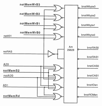
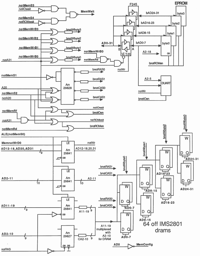
Note that during a refresh cycle, AD31 is low so that the CAS signals to both banks are disabled. Figure 10 shows the address decoding.
The notRAS and notCAS signals will need to be buffered because each is required to drive 32 DRAMs, giving a total load capacitance on each line of:
32 x 6 = 192 pF
The four notMemWrB strobes will also require buffering as, for a 2 Mbyte memory, they must each drive 16 DRAMs giving a total capacitive load on each line of:
16 x 6 = 96 pF
The maximum load specified by INMOS is 50 pF.
Neither of these figures allows for layout capacitance so the actual load will be somewhat more.
We will choose to gate the notMemWrB strobes with some address decoding, prior to buffering them, so that they are not enabled to the DRAM when writing to peripherals.
The address decoding requires that latched addresses should be valid as early as possible, and the most effective way to do this is with transparent latches. This way, the addresses will be stable before they are latched by notMemS0, so that the first stages of the decoding will already have settled. The complement of some of the address lines are also required by the decoding. These are provided by inverting the latched addresses.
The address multiplexing can be done by using an address latch with tri-state outputs and a tri-state buffer. The delayed RAS signal is used to switch between the buffer (row address) and latch (column address). Figure 11 shows the address latching and multiplexing circuit.
Since this is the most critical timing, and the one most subject to amendment, it should now be checked. This requires the drawing of a more detailed timing diagram than figure 9. The logic that has still to be added will not affect the timing.
The following steps then need to be followed to investigate the timing properly:
The following table will be useful in determining propagation delays:
| Device | Type | low-high in nsec | high-low in nsec |
| 74F00 | Quad 2i/p NAND | 6.0 | 5.3 |
| 74F02 | Quad 2i/p NOR | 6.5 | 5.3 |
| 74F08 | Quad 2i/p AND | 6.6 | 6.3 |
| 74F27 | Triple 3i/p NOR | 6.0 | 5.3 |
| 74F32 | Quad 2i/p OR | 6.6 | 6.3 |
| AM29828 | 10x inv. buffer | 7.5(14*) | 7.5(14*) |
All 0-70 degrees C, worst case, load 50pF, *load 300pF
The emerging family of FACT HCMOS logic has superior characteristics to the FAST devices listed above, and is preferable where available. One of its main attributes is the symmetrical propagation delays which make it particularly suitable for buffering transputer links.
For most other logic, note that inverting logic generally has marginally lower propagation delays; thus if a gate has to be buffered, an extra 1-2 nsec can be gained by using say a NOR + inverting buffer over an OR + non-inverting buffer.
An examination of the resulting diagram, figure 12, shows one possible problem immediately: the write strobe may not go high until after the data bus has gone tri-state, causing data corruption on write with some RAMs. This is not a problem with the IMS2801 which latches write data on the falling edge of CAS or Write, whichever is the later.
However, this potential problem can be completely removed by substituting a 74F32 for the 74F02 and removing the high-current buffer to reduce the propagation delay for the write strobes. The 74F32 can drive up to 180pF and the loading calculated in section 3.5, with an allowance for layout capacitance, is less than this. It is possible to use two 74F32s for each of the write strobes, one for each DRAM bank, to give lower propogation delays. This now provides the timing shown in figure 13.
The final selection of DRAM device can now be made. In this circuit RAS is used to switch the multiplexer and, since RAS goes high before CAS, the addresses supplied to the RAM will change before the end of the CAS access cycle. Therefore, we must use the IMS2801 which latches the column address on the falling edge of CAS, and is unaffected by subsequent changes.
The IMS280x series and most other DRAMs can perform two types of write cycle: early and late write. An early write cycle occurs when notWE is taken low before notCAS. Thus, the output buffers are turned off before CAS and the output pins remain tristate throughout a write cycle. A late write cycle occurs when notCAS is taken low before notWE. Thus, the beginning of a late write cycle appears to the DRAM to be a read cycle and read data is gated onto the output pins; this would be used in complex memory systems for read - modify - write cycles.
Early write cycles allow the DRAM’s data input and data output pins to be directly connected to the AD bus. Late write cycles require the data output pins to be gated onto the AD bus through tristate buffers enabled by notMemRd.
In this application, there is no requirement for late write cycles and the circuit will be simpler if we can achieve early write. This may be difficult because, to achieve sufficient read data set up time and RAS/CAS lead time, the falling edge of CAS (notMemS2) has been pulled forward to the beginning of T3. Hence, if the memory interface is configured for early write, the notMemWrB strobes fall coincident with notMemS2; i.e. coincident with CAS.
However, the heavier buffering on notMemS2 means that notWE should become valid before notCAS and, because the early write set-up time (tWL1CL1) for the IMS280x series is only 0 nsec, the DRAMs will experience early write.
Thus, the DRAM’s data input and output pins can both be connected directly to the AD bus.
The DRAM circuit has now been worked through and it remains only to choose the refresh interval and add EPROM and peripherals.
For the IMS280x series all 256 rows must be refreshed within 4.4msec if data is not to be lost.
The memory interface program gives the time taken for 256 refresh cycles based on the input clock frequency and the refresh interval. In this example, with a 5MHz input clock, the longest refresh interval of 72 clockin periods gives 3.69 msec for 256 cycles, within the maximum of 4.4 msec allowed for the DRAMs used.
notMemRd is used to generate the EPROM chip select because, in the default memory configuration used to read the memory configuration word from ROM after reset, it is the only available strobe. notMemS2 is used to generate the peripheral chip select because, since it goes high at the beginning of T6, its low period is stretched by wait states; whereas the low period of notMemS1 is fixed. The address decoding shown provides one wordwide ROM/EPROM space and one I/O space.
The timing for a common medium speed EPROM is typically:
| t access | 200 nsec | access time |
| t ce | 200 nsec | chip enable time |
| t oe | 75 nsec | output enable time |
| t df | 60 nsec | output turn off (to bus float) |
Access, chip enable and output enable times can all be met by the use of wait states with the timing already derived. However, Tdf is another problem. Referring to figure 10 and 13, it can be seen that peripheral and ROM/EPROM enable timing will be the same as CAS except for the wait states inserted between T4 and T5. Thus Tdf is restricted to a limit of 0 nsec if the bus is to be tri-state by the start of T1, when the addresses are placed on it. Using notMemS2 directly, rather than buffered, which is possible if the loading is not exceeded, will give 12-15 nsec available, but this is considerably less than that required.
The Tdf of typical peripheral devices, such as the SCN2681 A DUART (DUal Asynchronous Receiver / Transmitter) is up to 100 nsec, compounding the problem.
There are two basic routes to a solution; the first is to rearrange the timing, but this will slow down the DRAM cycles as well, thus defeating the object of this design. The second is to use external buffers on the data lines connected to ROM and peripherals. The delay through these buffers must be taken into consideration when determining the number of wait states required.
If F245 buffers are used, these should be enabled by notMemRd or notMemWrB during ROM or peripheral access cycles. These strobes must be used because they are the only ones available in the default memory configuration after reset. The direction can be selected by the latched MemnotWrD0 signal. This is low during T1 and T2 of a write cycle and can, therefore, be latched in the same way as the address.
Thus, all that remains to be designed is the gating logic for the wait state generator. This must gate notMemS4 to MemWait during ROM access cycles, and notMemS3 to MemWait during peripheral access cycles; during RAM access cycles and refresh MemWait must be held low. notMemS4 is used as the wait state generator for ROM accesses because it alone will generate a suitable length of wait state in the default memory configuration after reset. The NAND gate is included in the address decoding for ROM and peripherals to ensure that wait states are not inserted in refresh cycles; when A20=1 and A31=0.
Figure 14 gives the full detail of the circuit, and although this represents a complex design by transputer standards, it is still very simple when compared to the support logic required for other processors in a similar system. Memory configuration data is taken from EPROM, on data line 0. Figure 13 shows the final timing, without the wait states for EPROM and I/O.
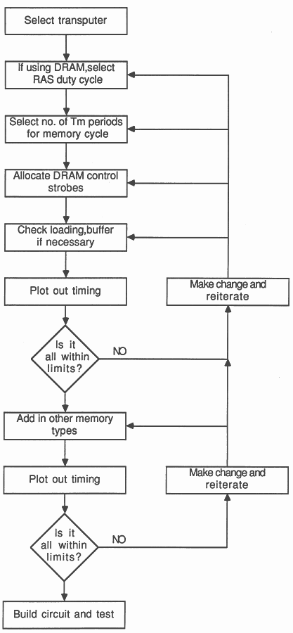
As each application will be different, generalising is hard, but figure 19 gives a flow chart showing the major steps. In all systems, it is necessary to start with the RAM timing, as that is the most critical area, and will have the greatest impact on system performance. In many designs, RAM is probably the only memory.
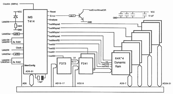
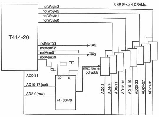
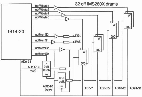
The example in figure 16 is taken from the Inmos B003 board. On this board, the 256k byte memory is made up of eight 64k x 4 DRAMs.
NotMemS0 is used to latch address bits 10-17 into a 74F373 and two 74F241s are used as an address multiplexer. NotMemS1 is used as notRAS, notMemS2 is used as the select on the multiplexer and notMemS3 as notCAS. Each notMemWB strobe goes to a pair of 64k x 4 DRAMs and notMemRD goes to all. Thus, the 256k bytes is organised as 64k words of 32 bits. The internal memory configuration selected by connecting MemAD5 to the MemConfig input is used; figure 17 shows the timing in terms of Tm periods, so the transputer clock speed has to be taken into account before actual timings can be added to the diagram.
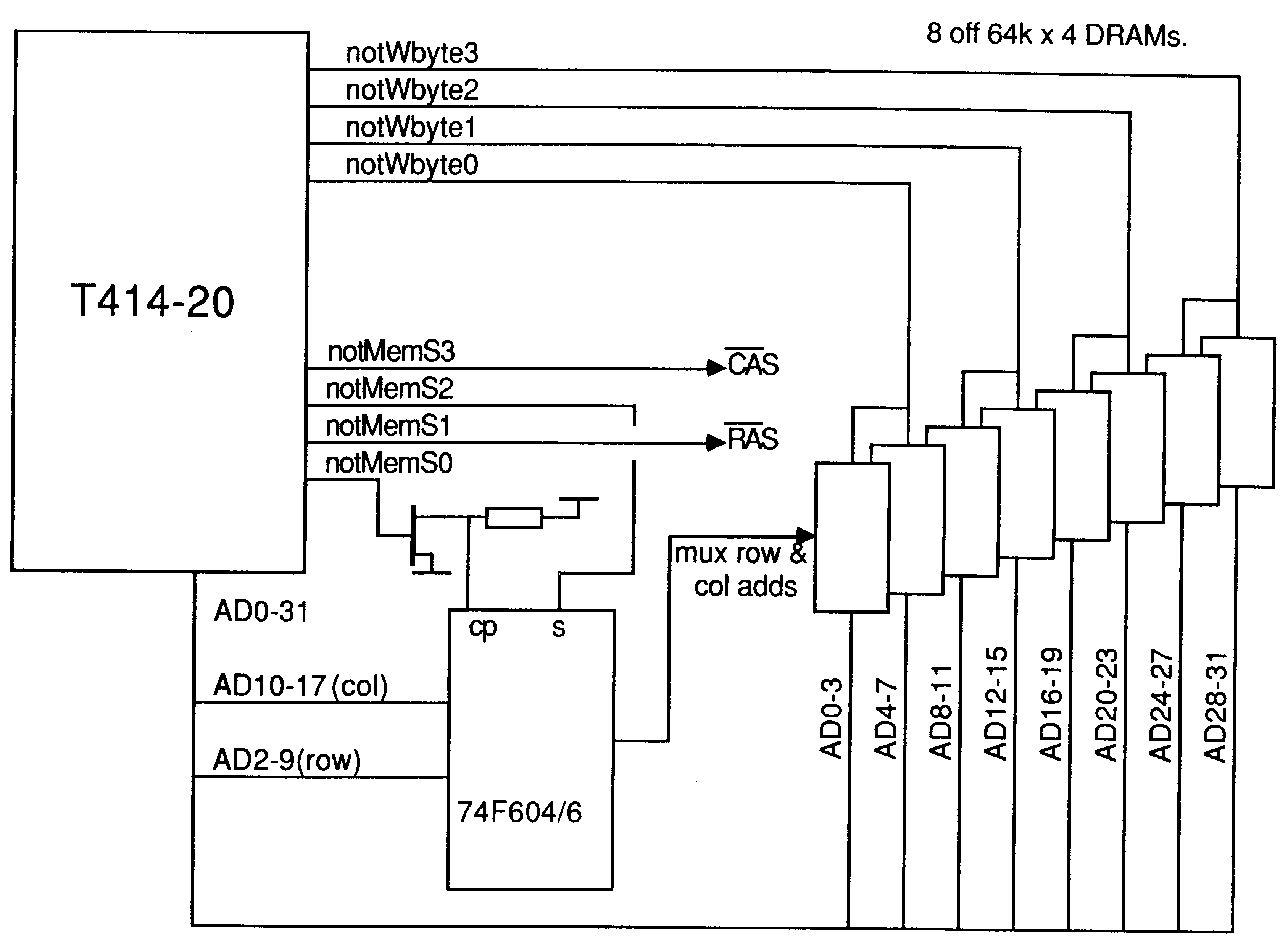
It is possible to reduce the component count still further by using devices such as the 74F604/6. This is a 16 bit latch to 8 bit multiplexed output, one version being faster and the other glitch free. The only drawback of this device is that the latches are rising edge triggered and, therefore, an inverter is needed in notMemS0. Again, care must be taken to ensure that the loadings on RAS and CAS are not exceeded. Figure 18 outlines this circuit.
In simple systems, the use of transistors or power MOSFETs can keep the required board area down. Power MOSFETs such as the Motorola MPF910 make useful drivers, as they come in a TO92 package, can handle peak currents in the range 1-2A, and have turn on/turn off times of 4 nsec; thus they can charge or discharge a large capacitance very quickly. The careful use of discretes such as these can allow better board layout and allows more control of the heavy currents that flow during switching.
This has been outlined during the main worked example, but is detailed here in its minimum form. The row and column address multiplexer is made from a tri-state latch and buffer. As this is a RAM only system, and there is only one bank of RAM, no address decoding is required and it is not necessary to detect refresh cycles. Instead, refresh cycles can be allowed to appear to the RAM as normal read cycles and they will still have the desired effect.
In the circuit shown in figure 19, RAS delayed by a gate is used as Amux. This allows CAS to go low one Tm period after RAS goes low, giving a longer access time and, hence, the shortest possible memory interface cycle time; 3 cycles of ProcClockOut. With longer cycle times, it is possible to use notMemS2 for Amux and notMemS3 for CAS. Note that to ensure early write, CAS has been delayed with respect to the write strobes by an extra buffer.
If very fast memory devices are available, it may be possible for CAS to fall at the beginning of T4 and still achieve a memory cycle time of 3 cycles of ProcClockOut. In that case, Amux can be generated by another strobe, as there will then be two Tm periods between RAS and CAS. This is shown by the circuit diagram, figure 20, and the timing diagram, figure 21.
The important parameters to consider here are the CAS to RAS lead time, the time from CAS going low to RAS going high, and the CAS access time. The CAS to RAS lead time is a minimum of 15 nsec for the 2800-60, adding the transputer tolerances to the strobe edges allows about 18 nsec; if a greater margin is required, inserting an extra buffer in RAS will provide it. For the 2800-60, CAS access time is 11 nsec maximum, so the buffer delay on CAS must be minimised to give sufficient access time. Thus, it may just be possible to do this with 2800-60 RAMs.
The circuit in figure 20 could be extended to 4 Mbytes by substituting 1 Mbit DRAMs for the 256k DRAMs but, with current memory speeds, 4 cycles would be needed for the memory interface.
Transputers can be booted from ROM (BootFromROM to Vcc) or from link (BootFromROM to ground). When booting from link, a header byte is expected, if it is in the range 2-255 it should be followed by that number of bytes. These will be placed in memory starting at MemStart ($80000048) and execution will then be transferred to this address. The code executes at low priority and its work space is located immediately above itself. Usually, this code will be a loader, to load the user’s program into this transputer and any others, if it is part of a network.
If the header byte is 0, a ”poke” operation will take place. The 0 byte should be followed by a 4 byte address (AAAA) and 4 bytes of data (DDDD) to be placed at that address:
input: header=0, then A A A A D D D D
|
If the header byte is 1, a ”peek” operation will take place. The 1 byte should be followed by a 4 byte address (AAAA). The transputer will then output, on the same link, 4 bytes of data (DDDD) read from that address:
input: header=1, then A A A A
output: D D D D |
After both the peek and poke operations, the transputer reverts to awaiting a new header (which could initiate another peek or poke).
Thus, if the user has another transputer, such as the one in the development system, it is possible to test the hardware by poking to the transputer under test to place data in the internal or external memory, and then peeking to read the data back and compare it. The same method can be used to test, say, a UART. These peek and poke operations allow simple test programs to be written in Occam and run on the development system, considerably simplifying the design engineer’s job. For temperature range testing, the system under test can be put in an environmental chamber with development system outside; all that is needed to connect them is a 4 wire link cable. In a mixed memory system, the engineer can now determine whether it is the memory or the DUART that is marginal, something that previously was difficult to do.
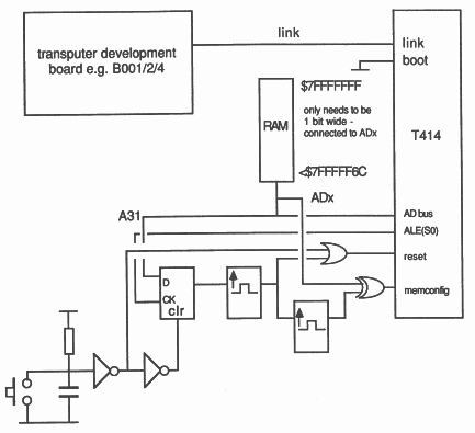
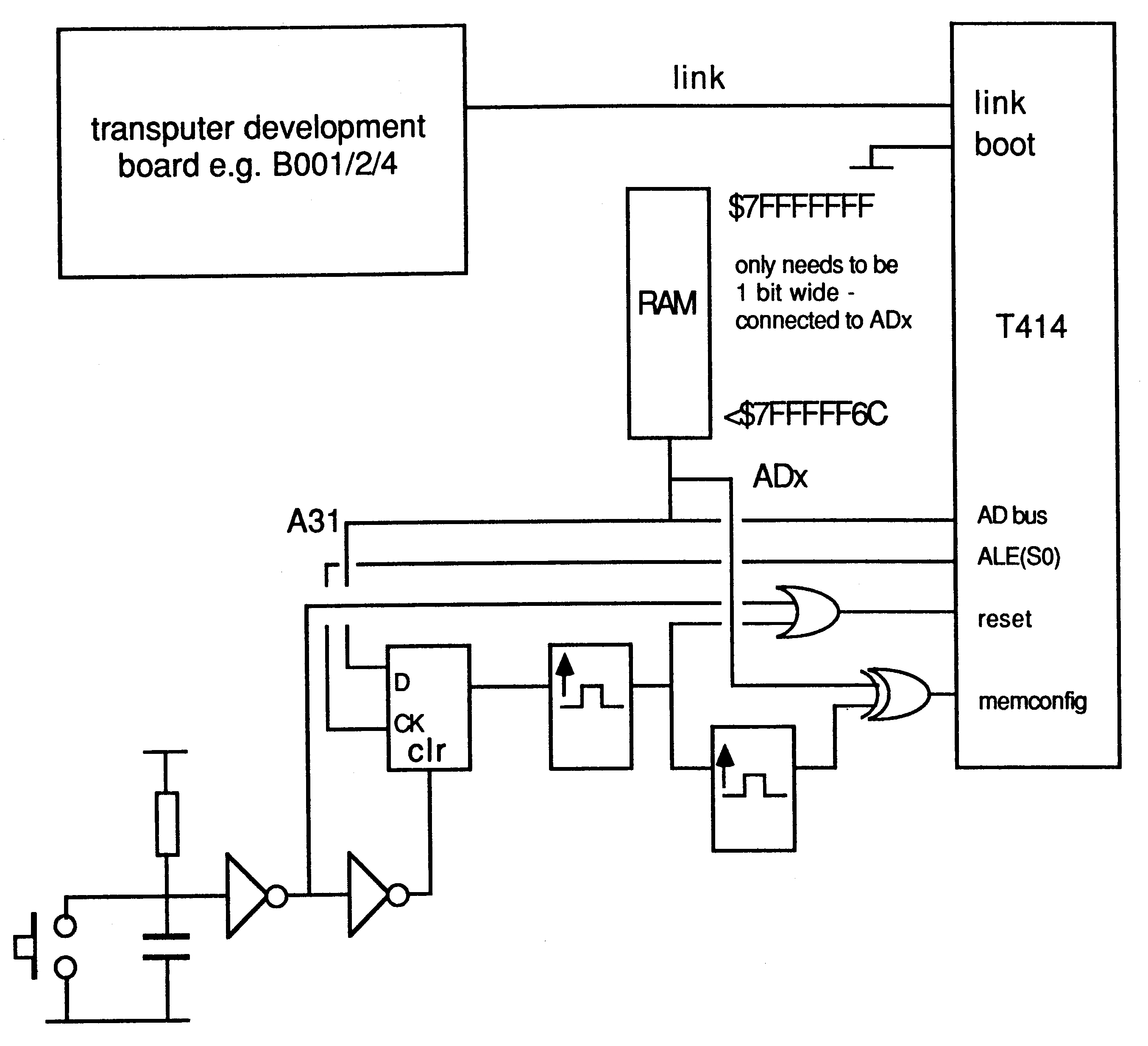
There may be occasions where a designer wishes to compare different memory interface configurations, and rather than programming an EPROM or a PAL in order to alter a parameter each time, software configuration for the memory interface would be useful. In figure 22, a basic scheme is outlined for this. It assumes that a known working transputer board is available, such as one that is part of the development system. This is used to ”poke” the required parameters into the RAM, which need only be one bit wide, as previously described for memory debugging; the memory configuration used is the internal configuration associated with ADx. Poking anything to a location of $8xxxxxxx will then generate a reset and cause the new memory configuration to be read from RAM on the line ADx. The memory debugging technique can then be used to test the system. Pressing the reset switch will generate a new reset and select the internal configuration again. Thus, once a software configuration has been selected, it cannot be altered by any program that may be run.
Whilst this first edition of this document has not covered every facet of the memory interface of the T414 transputer exhaustively, it has shown the basic features and how complex systems can be built with the minimum of effort. The reduced amount of logic required means fewer problems with propogation delays and race and, hence, faster memory cycle times. A number of helpful hints for the designers of transputer systems have also been included.