|
|
| IMS B004 IBM PC add-in board _____________________________________________________________________ |
| Stephen Ghee February 1987 |
To complement the launch of the Inmos Transputer in October 1985, a number of evaluation boards were designed, to allow the world to evaluate the performance / ease of use of the transputer. A number of hosts to control boards were considered, and the IBM Personal Computer was chosen, due to its wide usage, and large programming base. This article describes the design, implementation and uses of the board, both as an occam engine in development of Occam for transputer systems, and also the use of the board as an accelerator for computational intensive tasks that can be passed to the board from host programs.
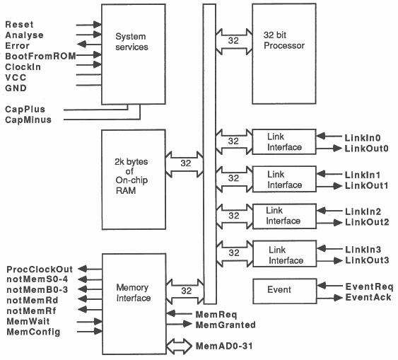
The transputer is a complete computer on a chip. There is a processor, a small amount of fast (50 ns cycle), on-chip static RAM, four serial communications ’Links’ (for external communications), and a programmable memory interface (which allows up to 4 Gbytes physical memory external to the transputer). The block diagram is shown in figure 1.
The transputer, and the programming language Occam, evolved together. Occam was designed to simplify the task of concurrent programming. Occam consists of three primitive processes, which are combined to create larger processes.
| v := e | assign the value of expression e to variable v |
| c ! e | output expression e to channel c |
| c ? v | input a value from channel c into variable v |
These primitives are combined to create processes using the occam constructors:
| SEQ | operate on the component processes in sequence |
| PAR | operate on the component processes concurrently |
| ALT | operate on the first process to become ready |
IF and WHILE constructs are also available. Each constructor is itself a process, and can be used inside other constructors to create larger processes. Concurrent processes, which cannot use shared resources, communicate across occam channels. These channels are single direction, point to point connections between processes, and give synchronised message communication.
Concurrent programming evolved as it became clear that many programs could be split into a number of tasks which could be operated on independently, and use some form of message passing for passing results, parameters, and synchronisation.
On standard sequential machines, implementing concurrency was solved by making the processor share its time between each task. This required a complex software ‘kernel’ to be written, which would control the switching of tasks (including itself) in and out of the processor, and handle the passing of messages. Switching the tasks frequently gives the user the impression that all of the processes are running simultaneously.
When developing occam programs on host machines such as the Personal Computer, an occam kernel is supplied to implement the concurrency and message passing via occam channels.
On transputers, the kernel has been implemented in hardware, giving a sub-microsecond task switch time, compared to a few milli-seconds on software driven multi-tasking machines. Occam processes can be mapped onto one transputer, which shares its time between them, or onto multiple tranputers, each taking a subset of the processes. The occam channels are mapped onto the tranputer links for processes on separate processors. In this way, programs can be developed on a single transputer, and extended to multiple transputers as more performance is required.
The tranputer’s links operate at 10MBaud, full duplex, and each link is capable of supporting two occam channels, one into the transputer, and one out from the transputer. Each link is implemented as an autonomous DMA (Direct Memory Access) engine, and so can perform communications with external devices as background tasks to the processor with negligible performance degradation.
There were three main elements required for the PC board.
Let us take the transputer and memory first. The first transputer available is the T414, a 32 bit processor, capable of 10 MIPS throughput.
The 32 bit multiplexed address/data bus of the T414 allows up to 4 GBytes physically addressable memory, external to the transputer, as well as the 2 KBytes fast static RAM on board the transputer itself. The memory map of the transputer is signed, with the internal RAM starting at the most negative address (Hex 80000000 to Hex 800007FF).The external memory starts at Hex 80000800.
For the Personal Computer add-in board, it was decided to give the user up to 2MBytes external RAM, mapped in to the negative half of the available address space, above internal RAM. For this amount of RAM on an IBM form-factor board, dynamic RAM (DRAM) had to be used. Also for such a large amount of memory, a parity checking system also had to be implemented.
The communication with the host Personal Computer is handled using an Inmos C002 Link Adaptor. This device can convert serial link data into byte-wide parallel data , and visa versa. The device allows simple interfacing with standard bus architectures, appearing to the host computer as a memory mapped peripheral.
A number of system control signals are also provided, which give the user the possibility of connecting a number of transputer boards to the add-in board via the Inmos links, and to allow the add-in board to control the system of transputers. All signals are software controlled.
In the following design, much of the logic required to control parity etc was implemented in PAL logic. In the design description, that logic is described in terms of the programming language used by the CUPL (Universal Compiler for Programmable Logic) programming system (available from Assisted Technology), available for Personal Computers.
To ease the task of designing memory systems, the transputer has an on board programmable memory interface. With this interface, it is possible to configure the external memory cycle of the transputer to be any width (to suit slow or fast memories), and a number of programmable strobes are supplied, which can be programmed to give signals such as RAS, CAS for dynamic memories. Automatic refresh, over a selectable refresh cycle time, can also be chosen. This eliminates the need to design complex timing generators, and so cuts down the number of devices required on the board.
To give up to 2 Mbytes of RAM on an IBM form factor board, 256Kx1 DRAMs were chosen. The memory interface needs to be configured to suit the cycle times of these devices. For evaluation purposes, parts with 150 ns access time were chosen.
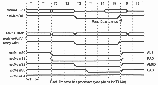
The external memory cycle is split into six states. These ’T states’ are as follows :
| State | |
| 1: | Address set up |
| 2: | Address hold |
| 3: | Read cycle tri-state/write cycle data setup |
| 4: | Extended for WAIT states |
| 5: | Read or write data |
| 6: | End tri-state/data hold |
The configuration of the cycle consists of specifying the number of each of these states that are required to give the timing needed by the particular memory device used. The memory interface is programmable to a resolution of a period ’Tm’, where Tm is the time for half a processor cycle. Any T State can consist of one to four Tm periods (The transputer has a Wait input which can be used to selectively insert more T4 states). The user programmable strobes are also defined with reference to Tm. A package is included in the transputer development system for calculating the configuration with reference to the memory device data sheets.
The parts used for the B004 were RevA transputers, with an 80 ns processor cycle, and so 40 ns is the minimum resolution the external memory cycle can be programmed to. For the 150 ns parts used for the memory, the following configuration was drawn up.
The refresh interval is set to give a refresh cycle every 4.32us. Early write cycles are used so that the Din and Dout pins of the DRAMs can be combined, and there is no need for buffering the data bus.
The transputer has a number of pre-defined configuration patterns that can be used, but the configuration described in figure 3 does not match any of these, so we must supply the configuration from an external device. For this particular board, a PAL was chosen, due to its small size, and number of functions available not only for the configuration but for other peripherals as described later.
The PAL is programmed as a finite state machine which responds to the addresses output by the transputer during the configuration stage. For each address, a data bit must be presented to the MemConfig input pin of the transputer. The bit pattern is split into 13 fields, which describe the number of Tm periods for the T States or user strobes, and refresh options. These fields are described in the memory interface section of the Transputer reference manual.
A number of requirements have to be met when using an external device to supply the configuration data to the transputer.
A karnaugh map was used to program the finite state machine. First, the chosen configuration must be put into bit form. The state machine (assuming the PAL will invert the data on the output pin) is programmed to respond (output a ’1’) for those addresses which have a ’1’ associated with them in the configuration data. For other addresses, the state machine does not respond (i.e. generates a ’0’ bit).
Table 1 shows the Karnaugh map, along with the decoded logic, associated with the configuration in figure 3.
|
MemConfig = A2 & A3 & !A4 & A5 & A6 & !A7 +
A2 & !A3 & A4 & A5 & A6 + A2 & !A3 & !A5 & !A6 & A7 + !A3 & !A4 & A5 & !A6 & A7 + A2 & !A3 & A4 & A5 & !A6 & A7 + A2 & !A3 & !A4 & !A5 & A6 & A7 + !A2 & A3 & !A4 & !A5 & A6 & A7 + !A2 & !A3 & A4 & A5 & A6 & A7 + !A2 & !A3 & !A4 & !A5 & !A6 & !A7 + A31 |
The last two terms are associated with the memory scan phase, and ensure that the state machine will respond during the scan phase (the inverter on the output of the PAL will then hold the MemConfig pin LOW). The scan phase involves each of the AD lines being pulled low in turn (and held low for the rest of the scan), starting with AD0. The AD31 term in the state machine ensures the MemConfig state is TRUE until AD31 is pulled low, when the term expressing lines AD2 to AD7 low will keep MemConfig state TRUE.
When the transputer enters the read cycle of the configuration stage, AD31 is always low, and the state machine responds to the addresses output by the transputer.
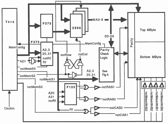
As the memory cycle of the T414 is a multiplexed address/data cycle, notMemS0 is used to latch the data (in IC14) from the PAL throughout the read cycle.
Program 2 includes the logic required to implement the state machine in a PAL (IC20).
Once the memory interface has been configured correctly, the logic for controlling the memory must be designed. As the memory interface controller on the transputer generates all of the signals needed, the only logic required are buffer and latch devices, the buffers used to multiplex the Row and Column addresses, and to drive the long PCB tracks along the memory array.
The circuit for the memory is shown in figure 4.
The transputer memory bus is a 32 bit, multiplexed address/data bus. The address is output during T2, and so we must latch the signals we require for the rest of the cycle. The address is a word address, and so MemAD0 and MemAD1 are used to carry information related to the type of cycle that is being executed. MemnotWrD0 signifies a write cycle when active, MemnotRfD1 signifies a refresh cycle. For this memory system, we need the MemnotRfD1 signal to disable CAS during refresh, and so this must be latched along with the column address needed for the DRAMs.
Two F373 transparent latches (IC14, IC15) are used to capture the signals needed, the latches being enabled by the falling edge of notMemS0 at the start of T2. At this point, we can be sure that the addresses are stable on the bus. At the same time, we can strobe in the row address (the low order address bits present on the bus during T2) to the DRAMs, using the notRAS signal derived from notMemS1.
Once the row address has been latched by the RAM, the column address (stored by the latches) must be presented to the RAM address inputs. When stable, the column address can be strobed in, using the notCAS signal derived from notMemS3. notMemS2 is used to perform the switching of the row-column addresses.
Two banks of 1 Mbyte each have been implemented. The banks are selected by one of two notRAS signals, these being decoded from the state of A20 (bank select address bit), A31, and the refresh signal given out on MemNotRfD1. The device used (IC7 - F153) is a dual multiplexer, each multiplexer outputting one of four inputs dependant on the state of the control signals A20 and A31. Table 2 shows the data output for values of these control signals.
| |||||||||||||||||||||||||||||||||||||||||||||||||
As can be seen, some of the inputs are controlled by notRf (latched from MemnotRfD1 by IC14). Normally high, this signal will only allow the appropriate notRAS signal (for the memory bank being addressed) to be asserted during a normal memory cycle. When notRf is active (low), both notRAS strobes will be asserted (for any address).
IC14 also latches an inverted MemnotRfD1 (Rf), which is used to control the generation of the notCAS strobes. Rf is OR’ed with notMemS3, so that if Rf is asserted (high), the output from the OR gate is always high, thus disabling notCAS. This makes use of the RAS only refresh facility of the DRAMs. The output from the OR gate is split and buffered to both banks of RAM.
A flip-flop formed from NAND gates (IC11) is used to create the non-overlapping strobe signals needed to switch the memory address from Row to Column. The flip-flop is triggered by the notMemS2 strobe.
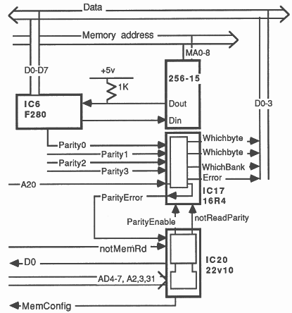
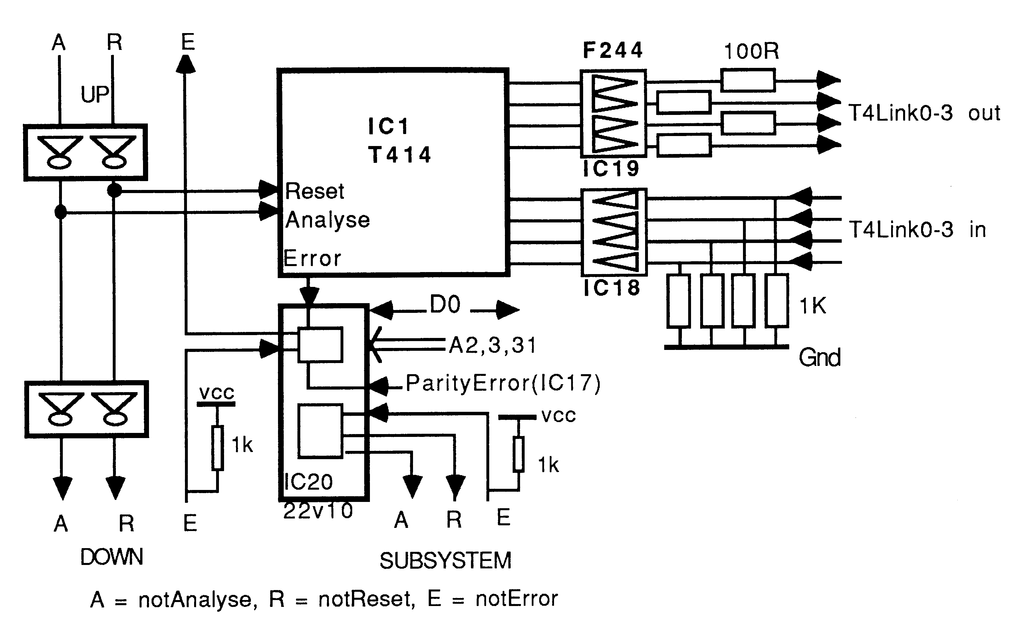
For such a large amount of dynamic memory, a parity checking circuit needed to be included. The transputer has overall control of the parity system, as the parity checker exists as a number of memory mapped registers. Simple memory accesses from processes allow parity to be enabled/disabled, the parity error flag read, and routing of the parity error flag to other transputers. Figure 5 shows the parity checking logic for one byte.
The parity control is handled by IC20. This PAL does the address decoding, and handles the registers that are available to the user processes.
For each byte in main memory, there is a parity bit stored in an associated addresses in the parity RAM. On a memory write cycle, each byte is converted to odd parity, the 9th parity bit being written to the parity RAM. On read, the parity bit for the particular address is passed into the parity checker, along with the byte from main memory, and parity checking takes place. If the parity is odd, the Parity(x) output signal (from the F280 parity generator/checker) will remain low. If an even parity situation is found, the Parity(x) signal will be asserted. This signal is read by the parity decoding logic in PAL IC17.
On memory read cycles, the four ParityError signals from the parity checkers are latched by IC17, and if parity is enabled (i.e. ParityEnable is asserted), the signals are decoded to indicate whether a parity error has occurred, and which byte and bank the error occurred in. The output lines of IC17 chosen for these decoded signals have tri-state buffers, which are enabled by the notReadParity signal from IC20, which is asserted when the transputer executes a read from the ParityError register. The logic required for the decoding of the four Parity(x) lines is given in Program 1.
If parity is enabled, then once a parity error has occurred, its state (i.e. byte, bank, error) will be latched, and no further parity errors will overwrite the first. Reading a parity error will not reset the parity latch, so the parity must first be disabled, a read cycle executed to clear the latch, then parity re-enabled. If parity is disabled, no parity errors will be reported. If a parity error has occurred (and parity is enabled), the ParityError output from IC17 is set. This signal can be combined with the main board error signal (see system control signals) under software control from the transputer.
IC20 is programmed to appear to the transputer as a number of registers. Three registers are used for parity control, these being
| EnableParity (write only) | Hex 2 |
| ParityToUp (write only) | Hex 3 |
| ParityError (read only) | Hex 2 |
(The addresses given are WORD addresses)
| |
Only bit 0 of the write only registers has any significance. Writing a ’1’ to either EnableParity or ParityToUp asserts the corresponding signal, a ’0’ de-asserts it. Reading from the ParityError register instructs IC17 to output the decoded data on the transputer data bus.
IC17 decodes parity error information onto data bits D0 to D3. The bits have the following significance.
| D0 | Error byte (low bit) |
| D1 | Error byte (high bit) |
| D2 | Error bank |
| D3 | Error |
If D3 is set, and parity is enabled, the byte and bank in which the parity error occurred can be calculated. The logic required to implement these registers is given in Program 2.
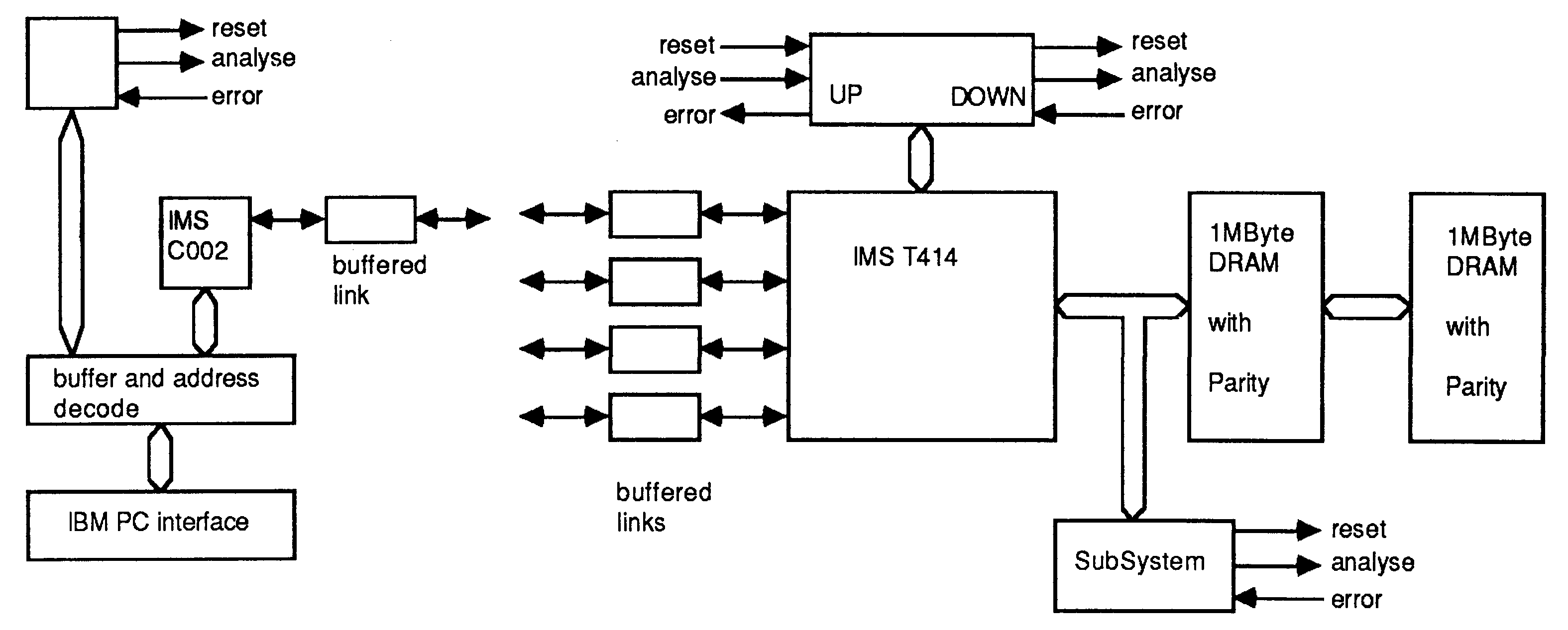
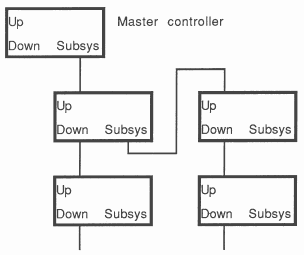
The board architecture, common to all Inmos transputer evaluation boards, allows any number of boards to be connected together to create a multi-processor system. On each board, the transputer links, suitably buffered, are brought to the edge connector, and cables are used to interconnect transputers on separate boards.
A number of control signals are also brought to the edge of the board, to provide control over the transputer’s reset, analyse and error functions. The system control signals are standard throughout Inmos transputer evaluation boards, and to understand the needs for the hardware to implement these control lines, the system architecture of the boards needs to be examined. Figure 6 shows how a hierarchical network of boards can be built into a large system.
The Up, Down, and Subsystem ports all carry the same control signals. These are
notReset and notAnalyse flow down the system (if the configuration of the system is considered to be as in figure 6), notError flows upwards. The notAnalyse signal is used to place the system into Analyse mode.
For a single board, there are two paths we must look at.
The schematic of the control system is shown in figure 7.
The architecture allows for any board in a chain to act as a master for another chain, allowing large systems to be split up into smaller subsystems, each with its own local controller. If an error occurs in the system, it can be handled be the local controller, without interfering with the rest of the system.
The link buffering is also shown. The four output links of the transputer are buffered using F244 buffer/drivers, and 100 ohm resistors (in series with the line). The input links are also buffered using F244 drivers. The inputs also have pull down resistors (1K ohm), which are used to prevent spurious inputs on the links being interpreted by the transputer as code or data.
The subsystem signals are handled by the 22v10 PAL IC20 (which handles the parity controls also). As with parity, the subsystem control is done via registers.
| SubsystemReset (write only) | Hex 0 |
| SubsystemAnalyse (write only) | Hex 1 |
| SubsystemError (read only) | Hex 0 |
(The addresses given are WORD addresses)
| |
Writing a ’1’ to bit 0 of SubsystemReset or SubsystemAnalyse asserts the associated signal, a ’0’ clears the signal. If bit 0 of SubsystemError is set, an error has been detected. Program 2 includes the logic required for these functions.
The logic required for the Up, Down ports is simple. The notUpReset and notUpAnalyse for the daisy chaining of boards enter the board from the Up port, are inverted (IC21) to give the correct polarity for the transputer Reset and Analyse, and are then inverted again for output at the Down port. The second inverter is used to provide the drive current required between boards. Both inputs (from the Up port) are pulled high with 1 K resistors to prevent spurious resets etc occurring when no external boards are connected.
The notDNError signal enters the board from the Down port, and is fed to IC20 (again, a 1 K pull up resistor is used to hold the line at the ’no error’ state when no other boards are connected). In IC20, the notDNError is combined with ParityError (from IC17) and the T4Error signal from the transputer, and fed out to the notUpError output of the board. The logic required to do this is given in Program 2.
The notUpError signal can inform the controlling board that some form of error has occurred, whether it be a parity error, transputer error, or an error from a board further down the chain.
The circuit described above gives a transputer with 2Mbytes of parity checked memory, four links to the outside world, and control signals. Although this is now able to communicate with any other transputer via the links, a means of communication with the host Personal Computer is needed.
The requirements for the interface was to have a parallel bus interface to the Personal Computer, and this parallel interface communicating with a transputer. There were two possible methods
The second method was chosen, as it maps onto the transputer concept of communications via occam channels. In this case, the host computer will appear as a process at the end of a channel mapped onto one of the transputers links. This method, however, means that the transputer selected to communicate with the host must use one link solely for this purpose.
To make this sort of interface possible, INMOS have also produced devices which convert parallel data into serial data, and vice versa, following the protocol of the Inmos links.
The IMSC002 link adaptor has a bi-directional 8 bit bus, to allow easy connection to standard bus architectures. A number of standard control lines, such as chip-enable, read/write and register select are included. The device takes parallel data, and converts it into serial form, and passes it out of the ’output link’. Incoming serial data is converted into parallel form, to be read by the parallel bus.
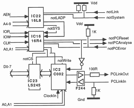
The circuit to perform the communications with the Personal Computer is outlined in figure 8.
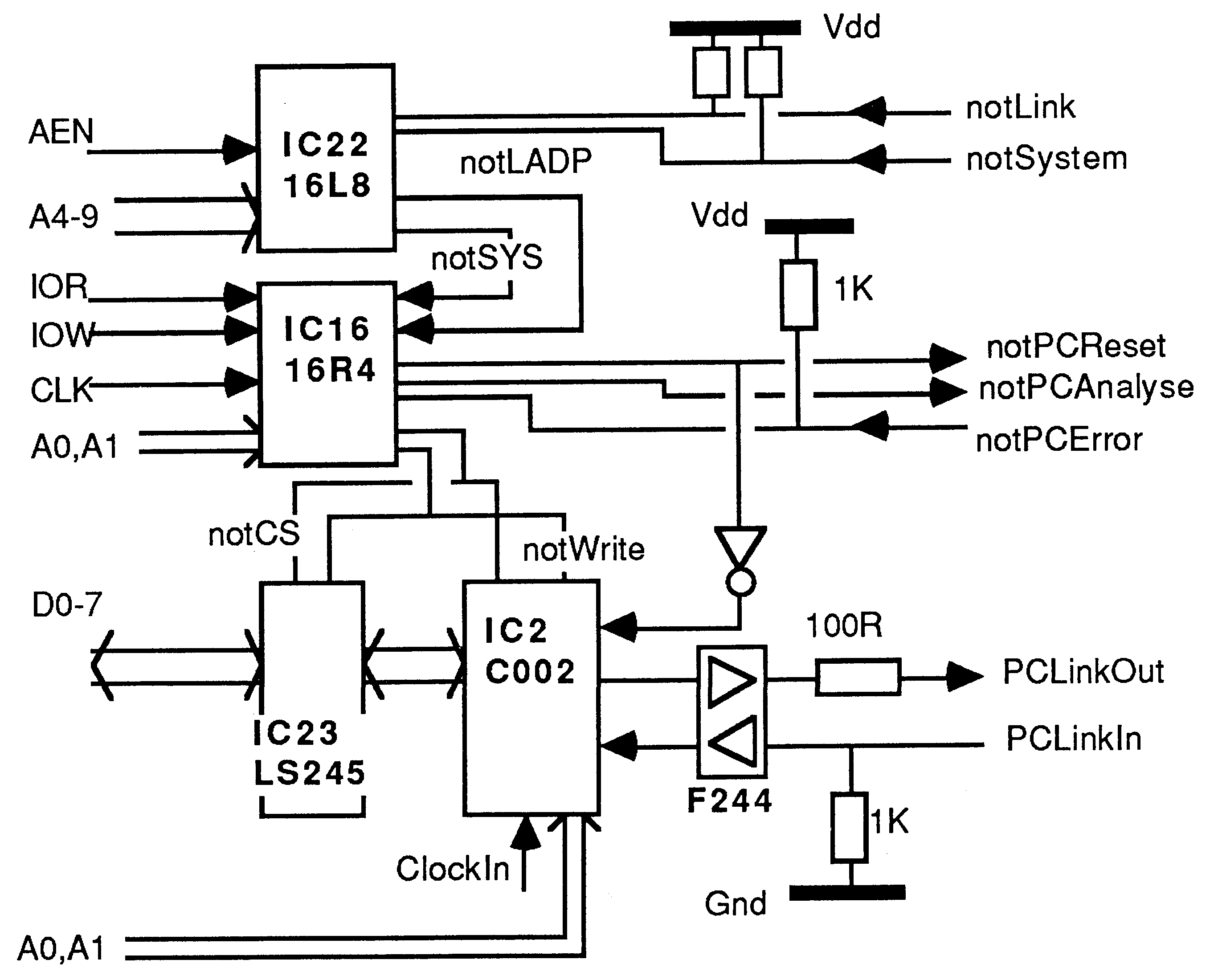
IC22 is a PAL which handles the address decoding from the bus. A4 to A9 are decoded, as well as AEN (when AEN is active, DMA controlled refresh is active on the PC bus, and so the board must be de-gated from the bus). Using a PAL for the address decoding allows the board address to be altered by changing the PAL. The board is currently located at address HEX 150 - 163 in I/O address space.
IC16 generates the timing sequence for the link adaptor from the clock and strobes generated from the Personal Computer.
Also included at the Personal Computer interface are more system control signals, which operate in the same manner as the transputer subsystem signals, but controlled by the Personal Computer. This allows the Personal Computer to be the master system controller. These are also implemented by 1016, in a similar manner to the subsystem and parity logic in IC20.
To allow more than one evaluation board to be fitted within a host, a method of selecting only one link adaptor and system control circuit to respond to accesses by the host was required. This selection method would allow all other boards to have all four links available for general use.
To satisfy these needs, it was decided to take the link from the link adaptor to the rear of the board, and to use a jumper plug to connect a transputer link to the link adaptor. A mechanism is included which informs the decoding logic that the jumper plug is in place, and the board can respond to the Personal Computer. The system control signals (controlled by the PC) are also taken to the rear connector, using a jumper plug to connect to the Up port, and using a similar selection mechanism to the links.
The selection mechanism involves an input of the selection PAL (IC22) to be pulled low if one of the jumper plugs is inserted. Only if the line (notLink or notSystem) is low will the corresponding select signal (notLADP or notSYS) be asserted. This signal enables the logic in IC16.
If notSYS is asserted, IC16 will allow the Personal Computer to access the registers used to control the Reset, Analyse, and Error signals. These registers operate in a similar manner to the subsystem control registers.
Writing a’l’to bit 0 of PCReset or PCAnalyse asserts the associated signal, a ’0’ clears the signal. If bit 0 of PCError is clear, an error has been detected. Program 3 shows the logic required for these functions., and Program 4 shows the address decoding logic.
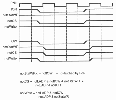
notLADP is used to select the link adaptor timing logic. Here, the IOW, IOR, and CLOCK signals from the PC bus are used to generate the access timing sequence for the link adaptor. This timing sequence, and the logic required to produce it, is shown in figure 9. The logic to perform this task is included in program 3, (with the address decoding given in Program 4).
Chip-Select (notCS) and the write strobe (notWrite) are also used to control the enabling and direction of the bi-directional buffer IC23 (LS245). Note notPCReset (after being inverted) is also used to reset the C002. This ensures that all links are reset before loading of the system takes place.
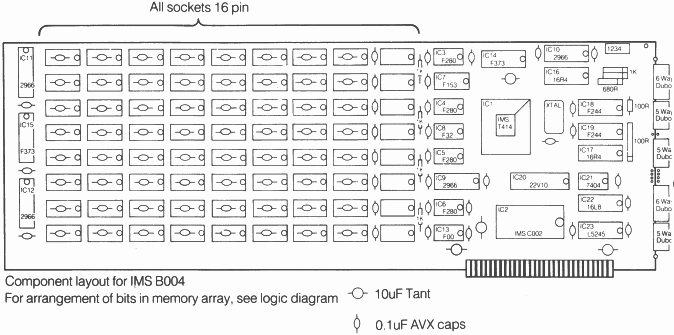
The component layout of the IMS B004 board is shown in figure 10. The memory array has been designed so that the MemAD lines flow from the transputer through the array, the addresses required by the RAMs are latched at the far end of the board, and buffered before being passed back down through the array. All devices have decoupling (the memory chips have their decoupling capacitors under the sockets). On the production B004, the capacitor required for decoupling the internal PLLs has a value of 10uF, though for new boards a 1uF miniature ceramic is preferred.
The IMS B004 board was originally designed to use RevA T414-G12S components. Some minor bugs in this early revision of the device meant that a 25 MHz clock was required for the transputer (not the 5 Mhz clock as is now standard). Also, a C003 link adaptor (which can be switched between C001 and C002 modes) was used in C002 mode. This also uses the 25 MHz input clock.
For current designs, the RevB T414 should be used. This is available in 15, 17, 20 MHz versions. This device has no known bugs. Note that there is a slight pin change from the RevA part, where CapPlus and CapMinus have been swapped (the full pin list is given in the Transputer Family document, available from Inmos). Also, a 24 pin 0.3” C002 package is available, to be used instead of the C003.
The new transputer devices have had the link circuitry updated to allow data transmission at 20Mbits/sec. If the designer wishes to make use of this link speed, a number of minor changes will have to made to the design given.
Use of a faster transputer (such as a T414B-G20S) will require some changes to the board. Where FAST devices have been used throughout the memory interface logic, FACT devices may now have to be used to make use of the low propagation delays (typically 2-3ns).
NOTE: 100 ohm serial resistors also need to be used to dampen the edges to prevent undershoot.
Fast DRAMs can also be used, and the memory configuration altered as these parts dictate. Using the new family of Inmos 280x fast DRAMs (with access times down to 60ns), the transputer can be run with no wait states (the memory interface cycle being three processor cycles).
If a faster memory cycle is to be chosen, care should be taken to ensure devices such as the memory address latches, drivers, and parity checkers do not create timing clashes due to propagation delays etc.
As the transputer can be programmed to supply all the timing signals necessary to build an external memory system, the design of a transputer system consists mainly of latching and buffering address, data, and control lines to provide sufficient drive current to take board capacitance etc into account. Practical things to note are the use of pull up or pull down resistors on all inputs of the board. Output links have a series resistor used for line matching (approx. 47 ohm). The input links require pull down resistors (approx. 100K ohm), to prevent floating inputs from being interpreted as code or data. All of the control signals (Up, Down, and Subsystem) are active low, so pull up resistors are required on all inputs to the board, to protect against lines not being used from floating.
All devices should have adequate decoupling capacitors near (on the IMS B004, the decoupling capacitors for the RAM array were inserted below the RAM sockets, saving board area).
The interface described above is that used to communicate with a Personal Computer bus. The IMSC002 can be interfaced to any parallel microprocessor type bus, and this would require a small change to the timing logic (implemented in a PAL).
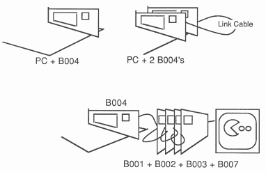
As stated at the start, the IMS B004 add-in board was primarily designed to complement the Personal Computer as an occam development station. Any number of evaluation boards can be connected to the board via the links. Figure 11 shows a few examples of large, parallel processing systems connected to a Personal Computer.
Programming the board for specific applications is done using the transputer development systems, using Occam. In the near future, it will also be possible to program the transputer system in ’C’, Pascal, and Fortran, as well as Occam. With these language compilers, it will be possible to take existing algorithms, and re-compile them for transputer applications. Also, by using Occam as the harness to describe the concurrency of the system, it is possible to run multiple processes, which could be written in any of the four languages.
Other uses include using the board as a high-performance number crunching device, used as a slave processor to the host machine. Here, any application could be written (or a current application modified) to pass data to the board, which will perform certain tasks on that data, before passing it back to the host machine for displaying etc. The interface software sees the board as a number of memory mapped registers. For example, a high performance flight simulator could be written, the transputer system doing the complex trigonometry involved with aircraft position, windowing, 3D-2D conversions, passing vector information to the host computer for display. By using multiple boards, the tasks could be split between many processors, giving orders of magnitude improvement in performance.
PARTNO IC17 ;
NAME PARITYPAL ; REVISION 01 ; DATE 14/10/85 ; DESIGNER S.Ghee ; COMPANY Inmos Limited ; ASSEMBLY B004 ; LOCATION 16R4 ; PIN 1 = !notRD ; PIN 2 = nc2 ; PIN 3 = Parity0 ; PIN 4 = Parity3 ; PIN 5 = Parity1 ; PIN 6 = A31 ; PIN 7 = Parity2 ; PIN 8 = A20 ; PIN 9 = EnableParity ; PIN 11 = !notReadParity ; PIN 12 = nc12 ; PIN 13 = ParityError ; PIN 14 = PStat0 ; PIN 15 = PStat3 ; PIN 16 = PStat1 ; PIN 17 = PStat2 ; PIN 18 = nc18 ; PIN 19 = nc19 ; /* PStat0-3 are connected to bits 0-3 of the transputer data bus PStat0,1 represent the parity ’BYTES’ PStat2 represents the parity ’BANK’ PStat3 signals a parity error Once a parity error has occurred, it is latched onto the outputs of the pal and no other errors are latched. If parity is DISABLED, the latches are reset. */ FIELD ErrByte = [PStat1..0] ; $DEFINE L ’b’0 $DEFINE H ’b’1 ErrByte.d = ([L, L] & Parity0 & !PStat3) # ([L, H] & !Parity0 & Parity1 & !PStat3) # ([H, L] & !Parity0 & !Parity1 & Parity2 & !PStat3) # ([H, H] & !Parity0 & !Parity1 & !Parity2 & Parity3 & !PStat3) # (ErrByte & PStat3) ; PStat2.d = A20 & !PStat3 # PStat2 & PStat3; /* For PStat3, clear if Parity disabled, but do not set if in top half or if no error */ !PStat3.d = !EnableParity # !PStat3 & EnableParity & !A31 # !PStat3 & EnableParity & !Parity0 & !Parityl & !Parity2 & !Parity3 ; ParityError = PStat3; |
PARTNO IC20 ;
NAME REVBCONFIG ; DATE 27/1/86 ; REV 01 ; DESIGNER S.Ghee ; COMPANY Inmos Limited ; ASSEMBLY B004 ; LOCATION 22v10 ; /******************************************************/ /* memory configuration , and subsystem reset etc PAL */ /******************************************************/ /** Allowable Target Device Types : PAL22V10 */ /******************************************************/ /** Inputs **/ PIN 1 = !notWRBO ; /* Register Clock */ PIN 2 = ParityError ; PIN 3 = !notSSError ; PIN 4 = A3 ; PIN 5 = A2 ; PIN 6 = A31 ; PIN 7 = T4Error ; PIN 8 = !notRD ; PIN 9 = !notDNError ; PIN 10 = AD6 ; PIN 11 = AD5 ; PIN 13 = AD4 ; PIN 14 = AD7 ; PIN 15 = AD0 ; PIN 16 = nc ; PIN 17 = !notUPError ; PIN 18 = !MemConfig ; PIN 19 = !notSSReset ; PIN 20 = !notSSAnalyse ; PIN 21 = EnableParity ; PIN 22 = !notReadParity ; PIN 23 = ParityToUP ; FIELD ADDRESS = [AD7..4, A3..2] ; FIELD SelAddr = [A3..2] ; FIELD output = [ notSSReset, notSSAnalyse , EnableParity, ParityToUP] ; /* Logic equations for 5 cycle memory. The items not commented out generate the bits as shown in the state machine diagram */ MemConfig = ADDRESS:[6C] # /*ADDRESS:[70] #*/ ADDRESS:[74] # /*ADDRESS:[78] #*/ /*ADDRESS:[7C] #*/ /*ADDRESS:[80] #*/ ADDRESS;[84] # /*ADDRESS:[88] #*/ /*ADDRESS:[8C] #*/ /*ADDRESS:[90] #*/ ADDRESS:[94] # /*ADDRESS:[98] #*/ /*ADDRESS:[9C] #*/ ADDRESS:[A0] # ADDRESS:[A4] # /*ADDRESS:[A8] #*/ /*ADDRESS:[AC] #*/ /*ADDRESS:[B0] #*/ ADDRESS:[B4] # /*ADDRESS:[B8] #*/ /*ADDRESS:[BC] #*/ /*ADDRESS:[C0] #*/ ADDRESS:[C4] # ADDRESS:[C8] # /*ADDRESS:[CC] #*/ /*ADDRESS:[D0] #*/ /*ADDRESS:[D4] #*/ /*ADDRESS:[D8] #*/ /*ADDRESS:[DC] #*/ /*ADDRESS:[E0] #*/ /*ADDRESS:[E4] #*/ /*ADDRESS:[E8] #*/ /*ADDRESS:[EC] #*/ ADDRESS:[F0] # ADDRESS:[F4] # /*ADDRESS:[F8] #*/ ADDRESS: [0] # A31 ; /* switch all Async resets OFF */ output.ar = ’b’0 ; /* switch all sync presets OFF */ output.sp = ’b’0 ; /* subsystem control logic */ notSSReset.d = AD0 & !A31 & SelAddr:[0] # notSSReset & !(!A31 & SelAddr:[0]) ; notSSAnalyse.d = AD0 & !A31 & SelAddr:[4] # notSSAnalyse & !(!A31 & SelAddr:[4]) ; AD0 = notSSError ; AD0.oe = SelAddr:[0] & !A31 & notRD ; AD7.oe = ’b’0 ; /* Parity control logic */ EnableParity.d = AD0 & !A31 & SelAddr:[8] # EnableParity & !(!A31 & SelAddr:[8]) ; ParityToUP.d = AD0 & !A31 & SelAddr:[C] # ParityToUP & !(!A31 & SelAddr:[C]) ; notReadParity = SelAddr:[8] & !A31 & notRD ; /* Error combining logic */ notUPError = T4Error # notDNError # ParityToUP & ParityError ; |
PARTNO IC16 ;
NAME IBM interface ; REVISION 01 ; DATE 14/10/85 ; DESIGNER S.Ghee ; COMPANY Inmos Limited ; ASSEMBLY B004 ; LOCATION 16R4 ; PIN 1 = Pclk ; PIN 2 = notPCError ; PIN 3 = !notSYS ; PIN 4 = nc4 ; PIN 5 = !notIOW ; PIN 6 = !notIOR ; PIN 7 = A0 ; PIN 8 = !notLADP ; PIN 9 = A1 ; PIN 11 = !outputenable ; PIN 12 = !notWrite ; PIN 13 = !notCS ; PIN 14 = !notStatWR ; PIN 15 = !notPCReset ; PIN 16 = !notPCAnalyse ; PIN 17 = nc17 ; PIN 18 = D0 ; PIN 19 = nc19 ; FIELD select = [A1..A0] ; /* Abbreviations */ readsys = notSYS & notIOR ; writesys = notSYS & notIOW ; readlink = notLADP & notIOR ; writelink = notLADP & notlOW ; /* IBM system control logic */ notIBMReset.d = D0 & writesys & select:[0] # notIBMReset & !(writesys & select:[0]) ; notIBMAnalyse.d = D0 & writesys & select:[1] # notIBMAnalyse & !(writesys & select:[1]) ; D0 = !notIBMError ; D0.oe = readsys ; /* Link adaptor timing logic StatWR is notIOW delayed by one PClk cycle */ notStatWR.d = notIOW ; notCS = writelink & notStatWR # readlink ; notWrite = writelink # notLADP & notStatWR ; |
PARTNO IC22 ;
NAME IBM address select ; REVISION 01 ; DATE 14/10/85 ; DESIGNER S.Ghee ; COMPANY Inmos Limited ; ASSEMBLY B004 ; LOCATION 16L8 ; PIN 1 = !notLink ; PIN 2 = A6 ; PIN 3 = A5 ; PIN 4 = A4 ; PIN 5 = ErrInt ; PIN 6 = nc6 ; PIN 7 = nc7 ; PIN 8 = !notAEN ; PIN 9 = IntInput ; PIN 11 = IntOutput ; PIN 12 = IRQ7 ; PIN 13 = A8 ; PIN 14 = A9 ; PIN 15 = !notLADP ; PIN 16 = !notSYS ; PIN 17 = A7 ; PIN 18 = !notSystem ; PIN 19 = IRQ6 ; FIELD IBMaddr = [A9..A4] ; notLADP = IBMaddr:[150] & notAEN & notLink ; notSYS = IBMaddr:[160] & notAEN & notSystem ; /* tri stated for the moment */ IRQ6.oe = ’b’0 ; IRQ7.oe = ’b’0 ; |