|
|
| Connecting INMOS links
__________ |
| INMOS Limited 72-TCH-018 |
The INMOS link is fundamental to the concept of the transputer and of occam [1, 2]. A link is the hardware implementation of an occam channel, each bi-directional link providing a pair of occam channels, one in each direction. A link provides serial data communication between two transputer family devices at speeds up to 20Mbits/s.
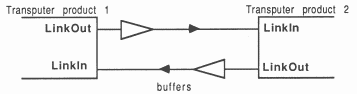
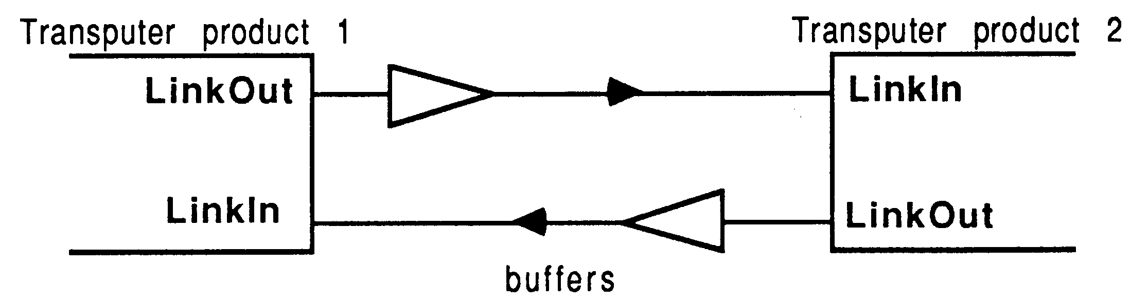
A link between two transputers is implemented by connecting a link interface on one transputer product to a link interface on the other transputer product by two uni-directional signal lines. Each signal line carries data and control information.
Communication through a link involves a simple protocol. This provides the synchronised communication of occam. The use of a protocol providing for the transmission of an arbitrary sequence of bytes allows transputer products of different wordlength to be connected together.
Electrically, link signals are TTL compatible and as such are a simple means of communication over short distances (< 0.3m). Links are designed for local communication. However, it is possible to use them over longer distances although a little more consideration is needed to ensure reliable operation. This application note is intended to provide the kind of information needed to engineer reliable links over various distances and media.
The note describes the operation of the INMOS link protocol followed by a discussion of the adverse phenomena encountered in link transmissions and means by which they may be overcome. Finally, a 5Mbits/s fibre optic link is described.
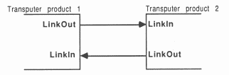
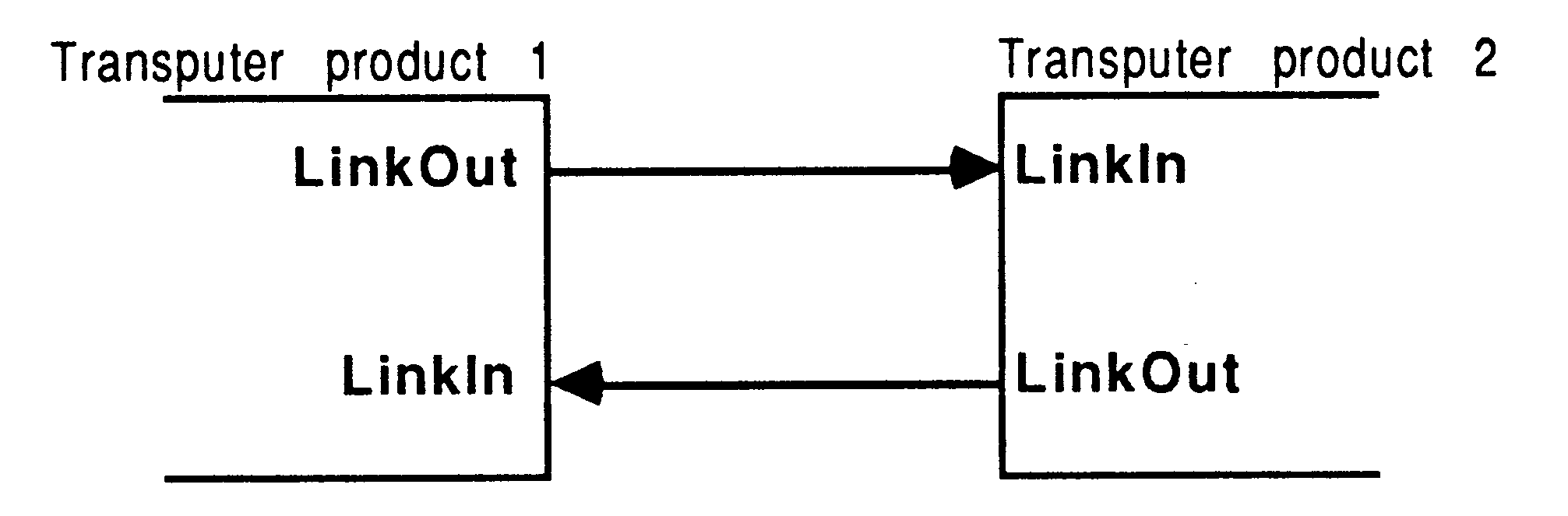
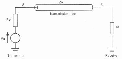
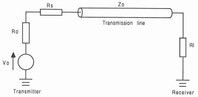
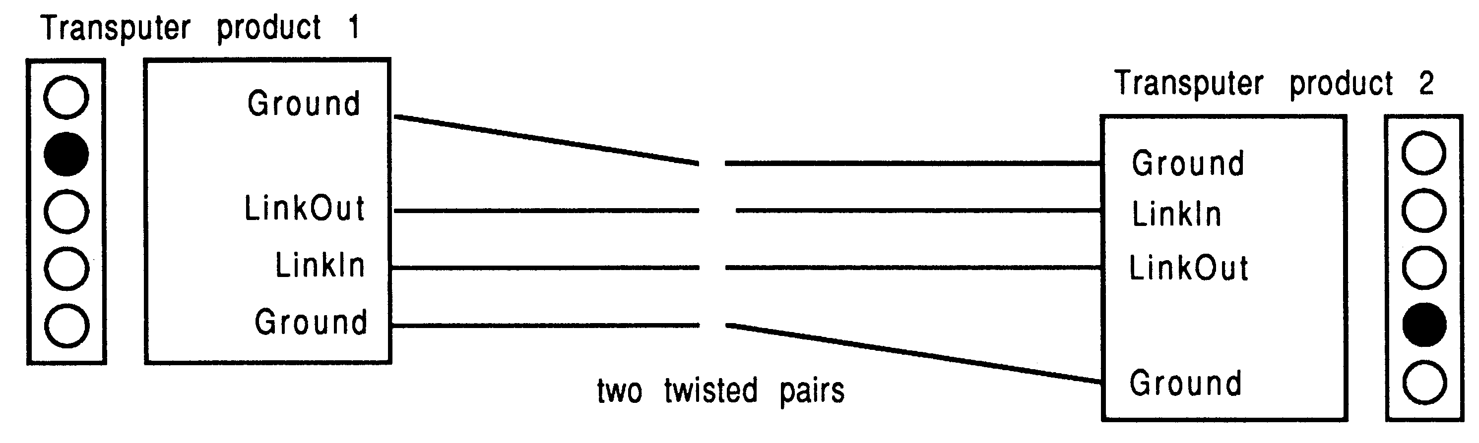
An INMOS link between two transputer products consists of two uni-directional signal lines connected to the link interface on each transputer family device, providing point-to-point serial communication, as shown in figure 1.
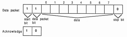
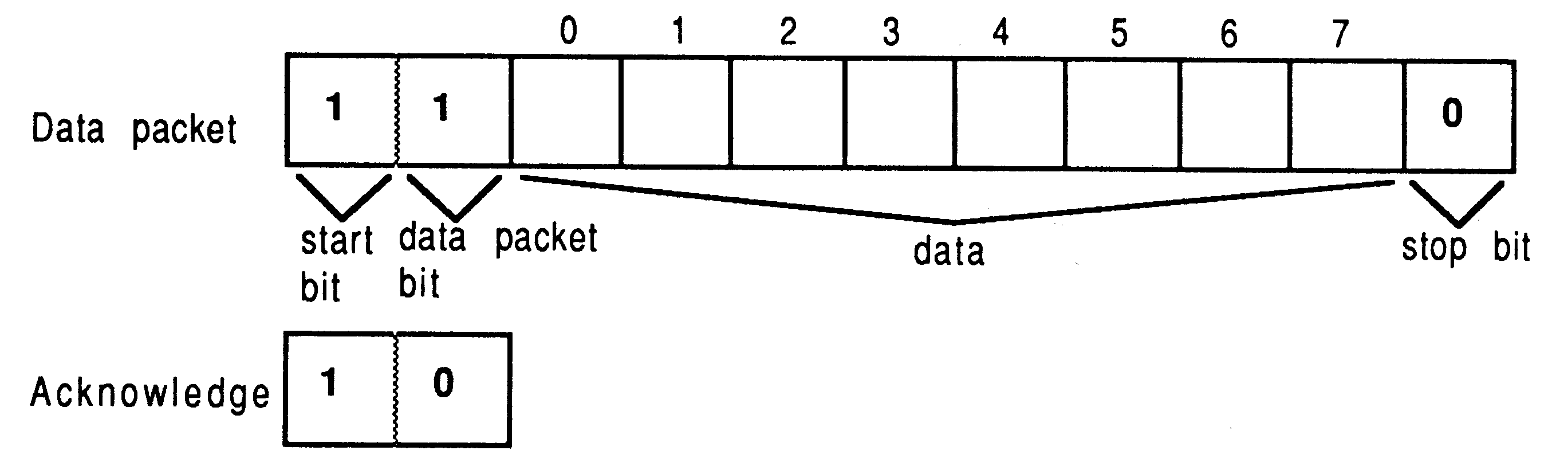
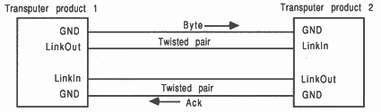
Communication across a link involves a simple protocol (figure 2).
Each message is transmitted as a sequence of single byte communications, requiring only the presence of a single byte buffer in the receiving transputer to ensure that no information is lost.
Each byte is transmitted as a start bit then a one bit, followed by the eight data bits and a stop bit.
After transmitting a data byte, the sender waits until an acknowledge is received. This consists of a start bit followed by a zero bit. The acknowledge signifies both that a process was able to receive the acknowledged byte, and that the receiving link is able to receive another byte. Acknowledges may not be sent in advance. The receiving end starts with an empty buffer, ready to receive the first byte. The sending link reschedules the sending process only after the acknowledge for the final byte of the message has been received.
Data bytes and acknowledges may be multiplexed down each signal line during duplex communication. In one implementation of the link (e.g. IMS T414) acknowledges are output on receipt of the full eleven bits of the data packet. The link implementation provided on the IMS T800 or IMS T222 allows overlapped acknowledges. In this implementation, the acknowledge may be sent immediately on receipt of the start bit and the ’data is to follow’ bit, allowing continuous data transmission with no delays between data packets.
The quiescent state of a link output is logic ’0’, i.e. 0V.
Links may be connected very simply over short distances (<0.3m). No engineering is required other than a direct wire connection between LinkOut of one transputer and LinkIn of another. The connection may consist of tracks on a PCB or backplane, or a cable.
Over greater distances, certain parameters of the interconnection medium must be taken into account:
A further consideration that applies to all link connections is protection of the link interface from electrostatic discharge.
This application note discusses these parameters as they apply to INMOS links. The communications medium commonly used at present by INMOS is twisted pair cable. The discussion of link parameters concentrates on this medium, but it could apply equally well to other transmission media, e.g. coaxial cable.
INMOS links are designed to transmit serial data between transputer family devices at speeds up to 20Mbits/s.
The signals are TTL compatible and as such are suitable for transmitting data over short distances (up to 30cm) with no engineering except a simple wire connection.
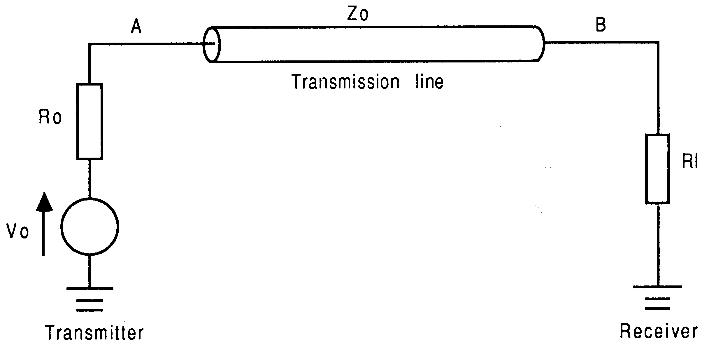
At greater distances, the wire will exhibit transmission line effects which can cause undesirable undershoot or ringing in the received signal.
This section discusses why these effects occur and means by which they may be alleviated.
Figure 3 shows a typical transmission system. As the length of the transmission line is increased signals travelling through it are delayed. Transmission line effects take place when the propagation delay is significantly greater than 33% of the risetime of the transmitted digital signals, manifesting themselves as ringing and undershoot, as shown in figure 4.
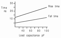
The 10-90% rise and fall times of the link outputs varies with capacitive loading, as shown in figure 5 [3].
As can be seen, the minimum rise time of 12ns corresponds to a capacitive loading of 20pF.
Transmission line effects become significant when the length of the transmission line is one tenth of the wavelength of the highest frequency component in the transmitted signal. i.e.
| l | = | 0.1λ |
| = | (0.1vptr(ns)) / (350 ∗ 106) |
Thus, the effects begin when the delay down the line is
| td | = | (0.1λ) / vp |
| = | (0.1tr) / (350 ∗ 106) | |
| = | tr / 3.5 | |
Where
| l | = | length of the transmission line (m) |
| λ | = | wavelength (m) |
| vp | = | propagation velocity of the signal through the line (m/s) |
| tr | = | rise time of signal (ns) |
Thus, for a rise time of 12ns, transmission line effects will occur when the delay down the line is greater than 3.4ns.
A typical value of vp for twisted pair cable is 60% of the velocity of light. Thus, a propagation delay of 3.4ns is equivalent to a length of 60cm.
Figure 5 shows that the fall time is generally half the rise time for a given capacitive load. Thus, the frequency components in a falling edge will give rise to transmission line effects when the line length exceeds half that of the rise time minimum length i.e. 30cm.
A transmission line has associated with it characteristic impedance, Z0. This is dependent on the inductance and capacitance per unit length and is given by
| Z0 | = | sqrt( Ll / Cl ) |
Where
| Ll | = | inductance per metre |
| Cl | = | capacitance per metre |
Consider a rectangular pulse sent along a transmission line. The rising edge of the pulse travels along the line arriving at the receiver after a propagation delay Td, determined by the capacitance and inductance of the line, and causes a voltage drop across the load resistance Rl giving rise to voltage vb. Depending on the value of the load resistance, a reflection may occur which will travel back down the line to the transmitter. The amplitude of the reflected voltage depends on the reflection coefficient, given by
| ρ | = | (Rl − Z0) / (Rl + Z0) |
The amplitude of the reflection is given by ρ ∗ vb. Clearly, if Rl = Z0, ρ is zero and no reflection takes place. In the worst case, if Rl ≫ Z0, ρ = 1; if Rl ≪ Z0, ρ = −1. If a reflection occurs, the reflected pulse travels back down the line arriving at the transmitter after another propagation delay Td. If the output impedance of the transmitter is not equal to Z0, another reflection takes place which travels back to the receiver where a further reflection takes place, and so on. The result is a series of reflections travelling back and forth along the transmission line each of which is successively smaller than the last. It is these reflections that cause ringing.
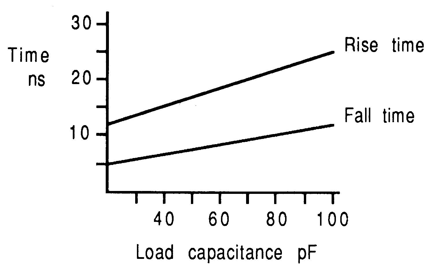
Figure 6 shows a simplified picture of the effect of a reflection on the transmitted signal. Figure 6(a) shows the waveform of the transmitted signal with the length of the transmission line at the critical length when the round trip delay (2Td1) is long enough to prevent the reflected waveform interfering with the transmitted waveform. In this case, ρ has a value of two thirds, the reflected pulse has a magnitude two thirds that of the transmitted pulse, shown in dotted lines, travelling in the opposite direction. Figure 6(b) shows the effect of the reflection interfering with the transmitted pulse where the round trip delay (2Td2) in this case is sufficiently small. If the load has a reactive impedance, the resulting waveform will exhibit capacitive and inductive effects. If the load is inductive, it will initially behave as an open-circuit, finally behaving as a resistance. Alternatively, a capacitive load will initially behave as a short circuit, then finally acting as a resistance. These effects will result in the reflected waveforms having time constants.
Ringing and undershoot are undesirable because they reduce the system noise margin. Some method of minimising undershoot is required. This is achieved by correct termination i.e. matching the impedance of the transmitter and/or receiver to the characteristic impedance of the transmission line. A simple method of termination that requires no DC power is series termination.
A resistor is placed in series with a transputer LinkOut pin such that the combined impedance of the resistor and the output impedance of the link pin is equal to the characteristic impedance of the transmission line. The resulting transmission system is shown in figure 7.
If Rl > Z0, the reflection coefficient at the load is
| ρl | = | (Rl − Z0) / (Rl + Z0) and 0 < ρl ≤ 1 |
If R0 + Rs = Z0, the reflection coefficient at the source is
| ρs | = | ((R0 + Rs) − Z0) / ((R0 + Rs) + Z0) |
| = | 0 |
This means that a transmitted signal will be reflected at the receiver, but the termination resistance will absorb the reflection, thus preventing any further reflections from reaching the load.
A single specified value of resistor will not be able to match the link output in all cases. The on-resistances of the P and N transistors of the link output are different and also vary between devices, with temperature and with supply voltage. Thus, a matching resistor may be specified to cope approximately with most variations.
Unless the transmission line is very well matched, the propagation delay down the line should not exceed 0.4 of the bit period at the operating link speed. Owing to the operation of the link output pad, a reflection arriving at the link output pin during a logic transition may cause a glitch on the local power supply of the link, possibly corrupting data.
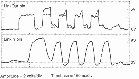
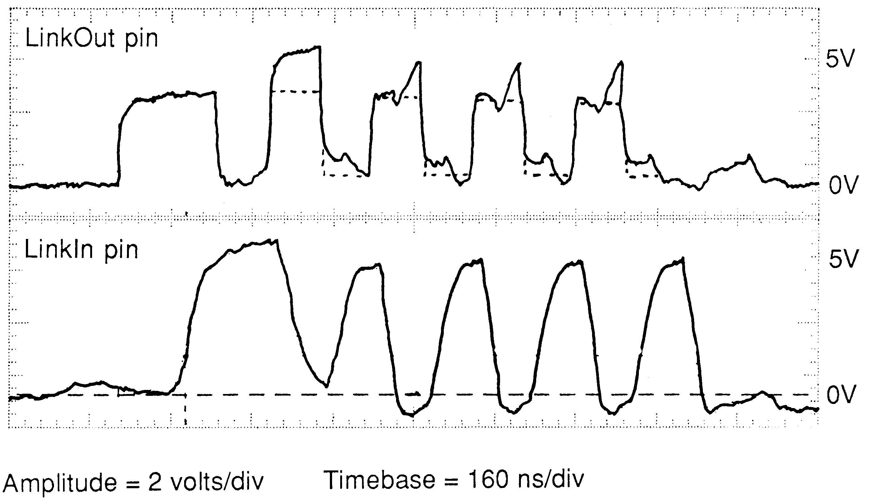
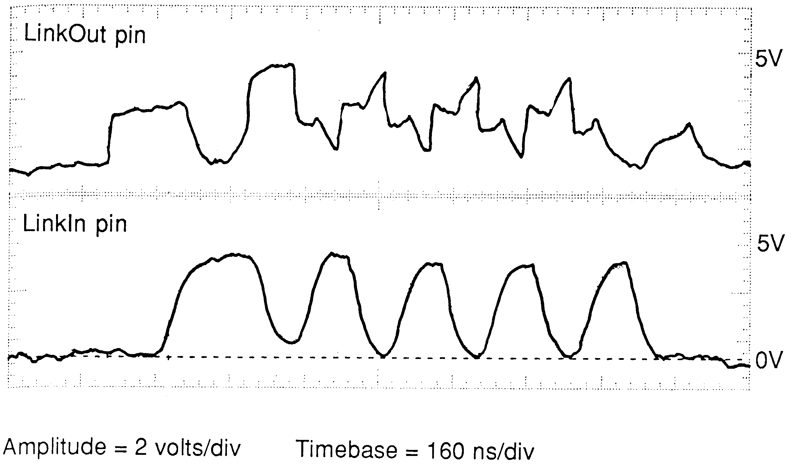
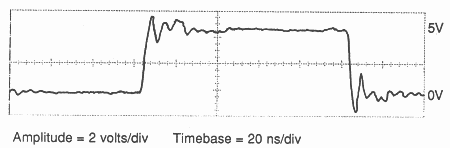
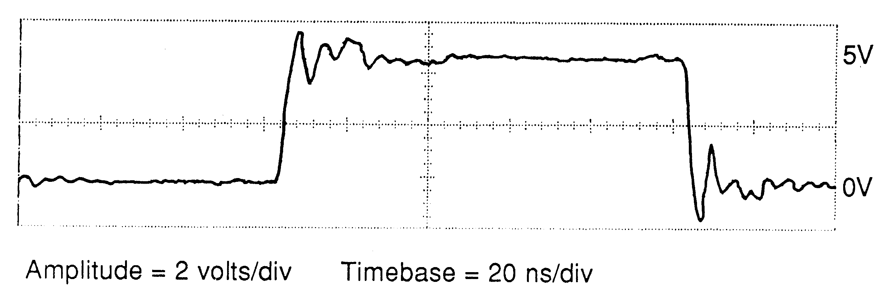
The oscilloscope plot in figure 8 shows a data byte transmitted at 10Mbits/s over 24 metres of 100Ω characteristic impedance twisted pair cable with no termination resistor. The top trace shows the waveform at the LinkOut pin. The reflections can be seen to arrive back at the sending end at a time twice the propagation delay later. The trace at the LinkOut pin is attenuated due to the effective potential divider caused by the resistances of the link output pad and the line. The dotted line shows the trace of the waveform, had there been no reflections. Thus, the reflections can be seen to be summated with the sending waveform, shown by the peaks on the data bits. The irregularity of the waveform is caused by the reactive load, discussed earlier in this note.
The bottom trace shows the received signal at the other end of the cable. Note the overshoot on the falling edges of the data bits caused by the signal being reflected a second time at the source.
The link interface inputs data by sampling each data bit 5 times, the correct value of the data being deduced as a result of these samples. Thus, excessive ringing may cause incorrect bit samples to be taken, corrupting data.
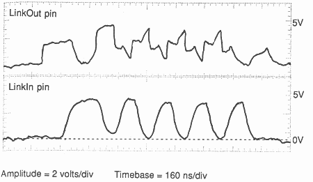
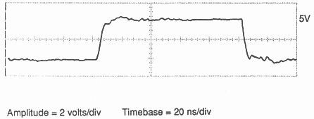
The plot in figure 9 shows the effect of inserting a resistance of 49Ω between LinkOut and the cable. The top trace shows that a reflection occurs at the receiver which travels back to the transmitter, in a similar manner to that shown in figure 6. However, in this case the termination resistor absorbs the energy of the reflection, eliminating a second reflection. The overshoot on the received signal, as shown in the bottom trace, is now eliminated. Since data will be switching between 1 and 0 regularly, there is a tradeoff between minimising overshoot and overdamping the signal. The value of the resistor required should be approximately 56Ω.
Series termination has advantages over other forms of termination (e.g. parallel termination). No power supply other than the logic supply is needed and the overall power requirement is low. Distributed loading along the line cannot be used, but since links are used point-to-point this is not a problem.
The link cables supplied with INMOS board products are made from twist ’n’ flat cable. This is 28 awg twisted pair cable with 2-inch flat sections every 18 inches to provide easy connector termination. The nominal characteristic impedance of this cable is 105Ω. A 56Ω series termination resistor provides good matching between the transputer and the cable.
Noise or electromagnetic interference (EMI) can come from numerous sources including lightning, electrical machinery and electrostatic discharges, any of which can cause interference on a communications line. Link signals are TTL compatible and as such have a specified noise margin when directly driving a TTL input:
| V OH(MIN) − V IH(MAX) | = 2.4 − 2 | ||
| = 0.4V | |||
| V IL(MIN) − V OL(MAX) | = 0.8 − 0.4 | ||
| = 0.4V |
i.e. noise on the line must be limited to 0.4V in order to avoid the possibility of unwanted changes in logic level.
Crosstalk occurs when signal lines are run close together. The changing signal in one line is coupled into the other line, appearing as a noise voltage which is proportional to the rate of change of the current in the first line, for inductive coupling. Noise produced by capacitive coupling is proportional to the rate of change of voltage.
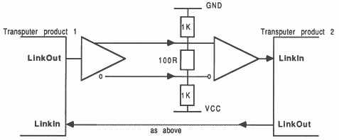
The protection of electronic circuitry from noise is a large subject [4], but some simple steps can lead to a reduction in noise pickup and crosstalk. Using twisted pair cable having a ground return twisted with each link signal line helps to reduce differential mode noise, i.e. noise which appears between the link signal and ground. Figure 10 shows the connections of an INMOS standard link cable. Note how each link signal line has its own ground. This also helps maintain constant characteristic impedance along the cable.
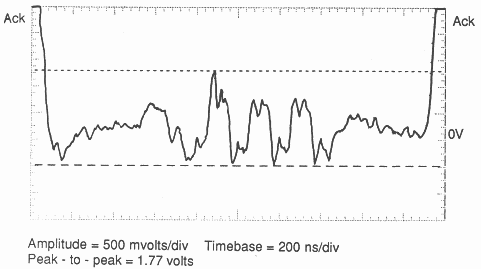
Screened twisted pair increases the immunity from common mode noise, i.e. noise coupled equally into both wires in a pair. Crosstalk can appear as common mode noise, depending upon the construction of the cable, and can be reduced by screening individual pairs. Figure 11 shows a test set up to record crosstalk between link signal lines. A process running on transputer T1 continuously sends the byte AA hex, i.e. bytes containing alternate ’1’s and ’0’s. Transputer T2 sends Acknowledge packets.
Figure 12 shows a plot of the crosstalk induced from the byte on T1 LinkOut0 onto T1 LinkIn0 when 10 metres of unscreened twist ’n’ flat is used. The peaks at the extreme edges of the plot are the acknowledge start bits. These peaks have been clipped by the oscilloscope in order to show the crosstalk on a reasonable scale. The crosstalk is caused by the rapid edges of the data packet bits in the other signal wire. It can be seen that the data packets are transmitted between acknowledges on separate fines.
The measurements are taken when transmitting at 20Mbits/s with no series termination.
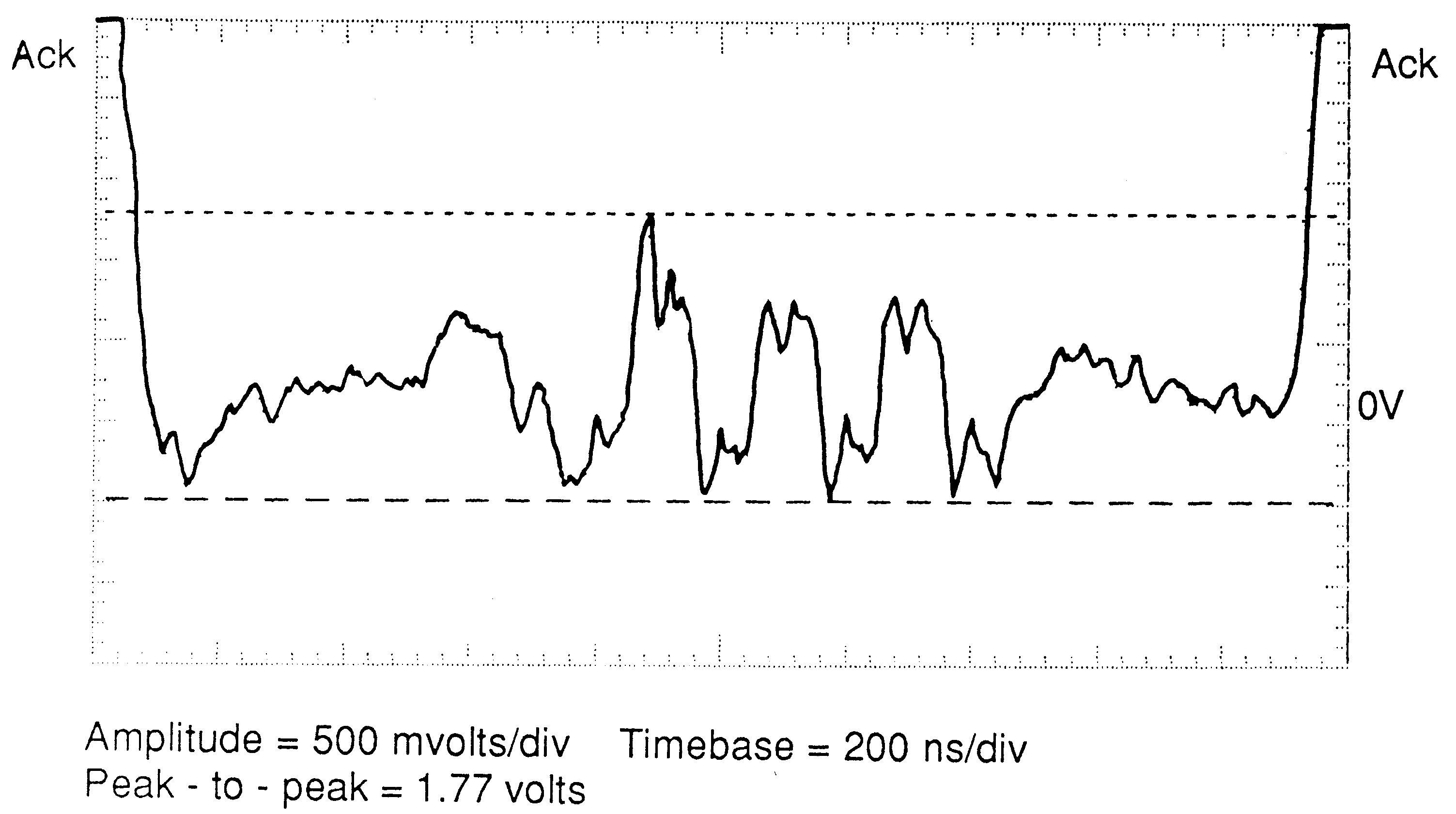
Figure 13 shows a similar plot using 18 metres of twisted pair where each pair is individually screened. Again, the two large, clipped peaks at either side of the plot are the acknowledge start bits with the data packet crosstalk being shown between the acknowledges. The dotted line on the inset trace shows the (exaggerated) waveform of the data packets on the other signal wire in order to show the correlation between the edges of the data packet and the crosstalk being coupled onto the other signal line.
The crosstalk is reduced from 1.77V to 760mV peak to peak, a reduction of more than 7dB due to the screening. A similar performance can be expected for external noise rejection. Since noise pickup increases with the length of line it is recommended that long links implemented with twisted pairs are screened. An overall screen is adequate, but individually screened pairs will improve the rejection of crosstalk. Screens should be connected to the frame ground at both ends of the cable, due to the high frequency components in the edges of the data.
Differential line drivers/receivers such as EIA Standard RS 422 [5], when used with twisted pair, provide maximum noise immunity. Because the signal is sent differentially common mode noise is rejected by the receiver up to its common mode rejection limit. Figure 14 shows an implementation of an RS 422 system suitable for use with INMOS links. This system has been used by INMOS for reliable link transmission over 160 metres of twisted pair at 5Mbits/s. It should be noted that the RS 422 specification limits the maximum bit rate to 10Mbits/s at a maximum distance of about 15 metres using 24 awg twisted pair. At 5Mbits/s, the maximum length is about 25 metres. The RS 422 specification is, however, deliberately conservative.
Assuming a noise free environment, the maximum length of line over which a link signal may be transmitted without buffering is determined by the attenuation of the line. Attenuation of twisted pair increases with the frequency of the signal transmitted along it. The bandwidth required for transmission of the significant frequency components of the link signal line spectrum can be expressed by
| f3dB | = | 350 / 6(ns) |
| = | 58MHz |
where f3dB is the frequency at which the line spectrum components are decreased by 3dB i.e. 50% of the initial magnitude, assuming a minimum fall time of 6ns.
This arises from the fact that high frequency components are attenuated more than low frequency ones, resulting in slower edges and the height of the corners of a signal is being reduced.
For a maximum signal reduction of 0.4V from the logic 1 level, the permissible attenuation is
| dB | = | 20 log ( V 1 / V 2 ) |
| = | 20 log ( 2.4 / 2 ) | |
| ≃ | 1.6dB |
The maximum line length is then
| lmax | = | 100m ( 1.6 / Atten ) |
where Atten is the cable attenuation in dB/100m at the operating frequency. For example, using twisted pair with an attenuation of 30 dB/100m at 58MHz.
| lmax | = | 100m * 1.6 / 30 |
| = | 5.3m |
This value is of course the maximum length of cable which will allow all frequency components up to 50MHz. The received signal will still be adequate, regardless of the rounding effects of the low pass filtering action of the cable. From figure 5, a link with a capacitive load of 80pF will have a fall time of 10ns. This corresponds to a maximum frequency component of 35MHz. For a cable with an attenuation of 18dB/100m at 35MHz, the maximum length of cable is 8.9m.
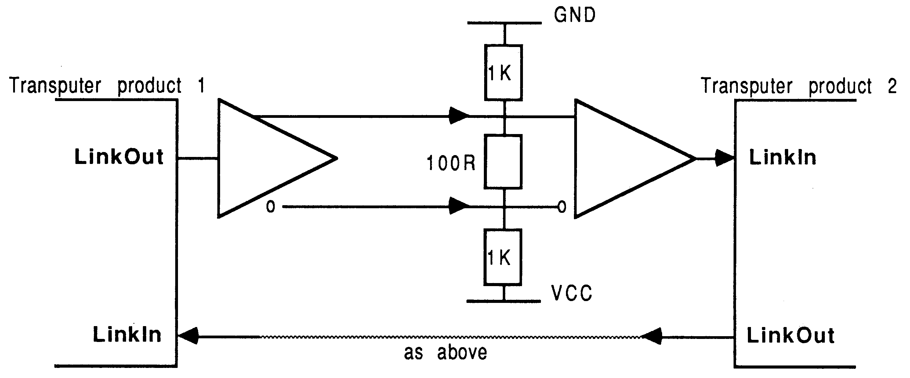
If longer links are required buffer/line drivers may be used (figure 15). Because of the asynchronous operation of links, the round trip propagation delay is unimportant as far as reliability is concerned. It is, however, important that the skew introduced by the buffers is less than the maximum skew quoted in the Transputer Reference Manual [1]. (Skew is discussed further in the next section.) To minimise skew and to maximise noise margin at all link speeds it is recommended that FACT buffers are used [6], e.g. the 74AC244 octal buffer/line driver.
| V CC | = | 4.5V |
| V OH | = | 4.4V |
| V IH | = | 3.15V |
Therefore
| Attenuation | = | 20 log ( V OH / V IH ) |
| = | 20 log ( 4.4 / 3.15 ) | |
| = | 2.9dB |
Hence
| lmax | = | 100m * 2.9 / 18 |
| = | 16m |
assuming the same cable as previous examples.
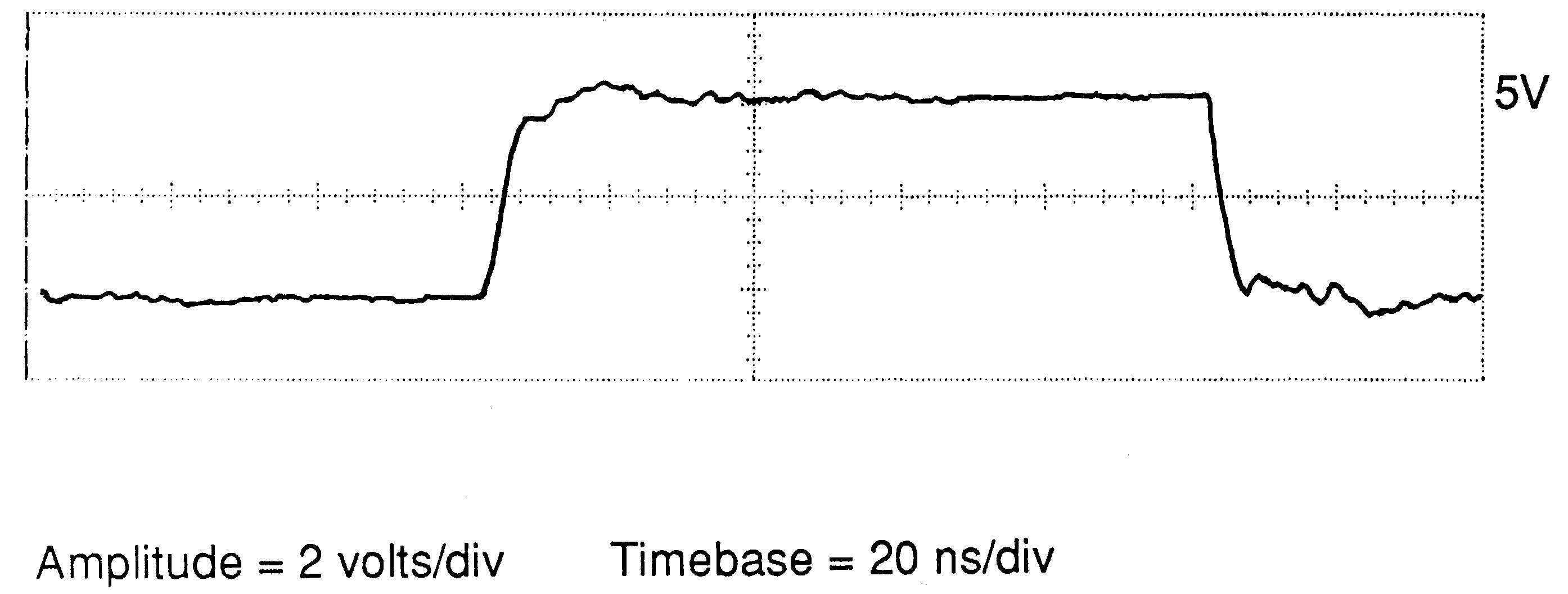
While the FACT data book states that the input and output diode clamps on a FACT device will match most transmission line impedances, it is recommended that a series matching resistor is used at the buffer output. The series resistor should be equal to the characteristic impedance of the transmission line. Figure 16 shows a plot of a bit taken at LinkIn in figure 15, operating at 10Mbits/s along a 50cm INMOS link cable. No termination resistor is used and ringing results. Figure 17 shows a similar plot taken after the insertion of a termination resistance of 91Ω which damps the ringing.
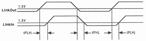
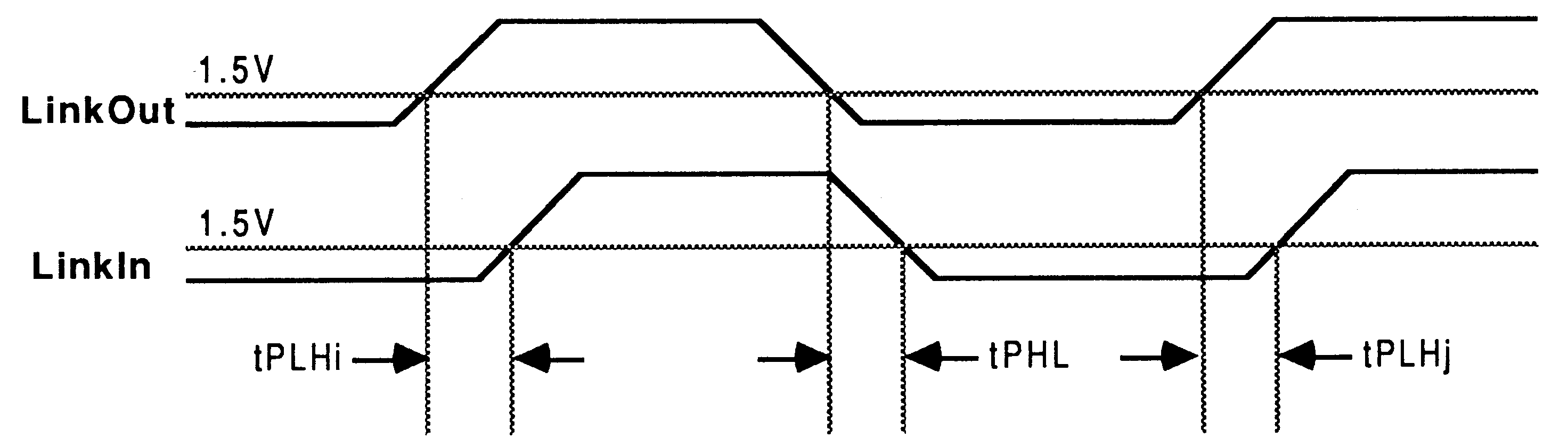
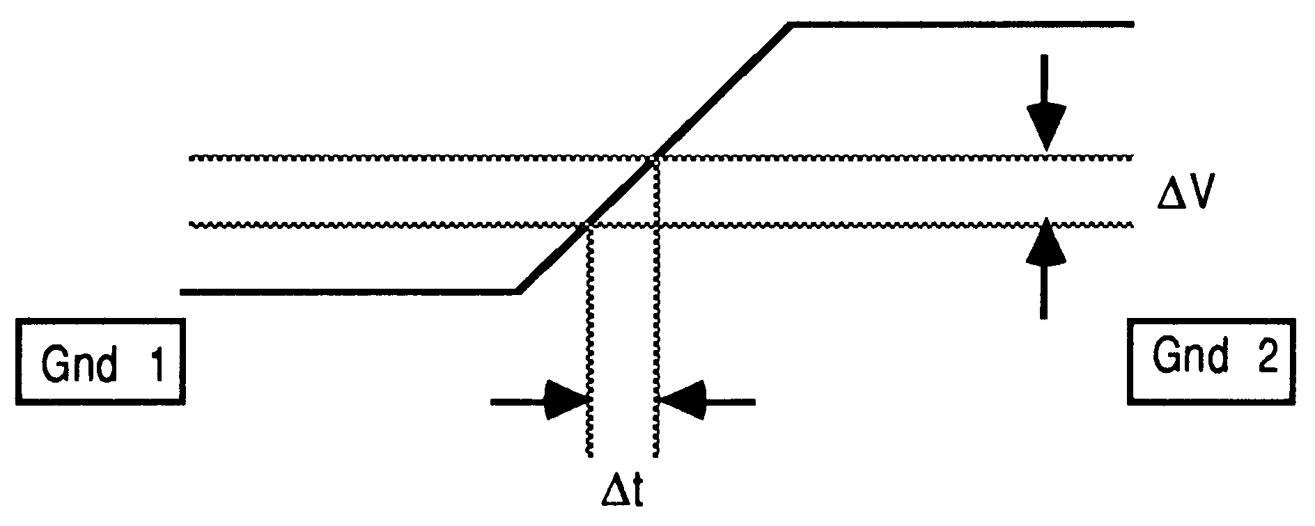
The skew of a system is defined as
| skew | = | max( |tPLH - tPHL|,|tPLHi - tPHLj| ) |
where tPLH is the system propagation delay for low to high signals, and tPHL is the propagation delay for high to low signals. The rising edge of a start bit is denoted by tPLHi and tPHLj relates to successive rising edges. The effect of skew is to broaden or narrow digital signals in the system. This changes the times at which data bits and the stop bit (and the next start bit) are seen at the receiving end relative to the leading edge of the start bit, shown in figure 18.
Skew varies instantaneously with power supply variations.
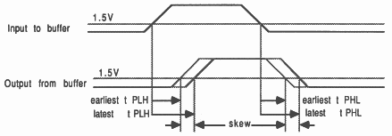
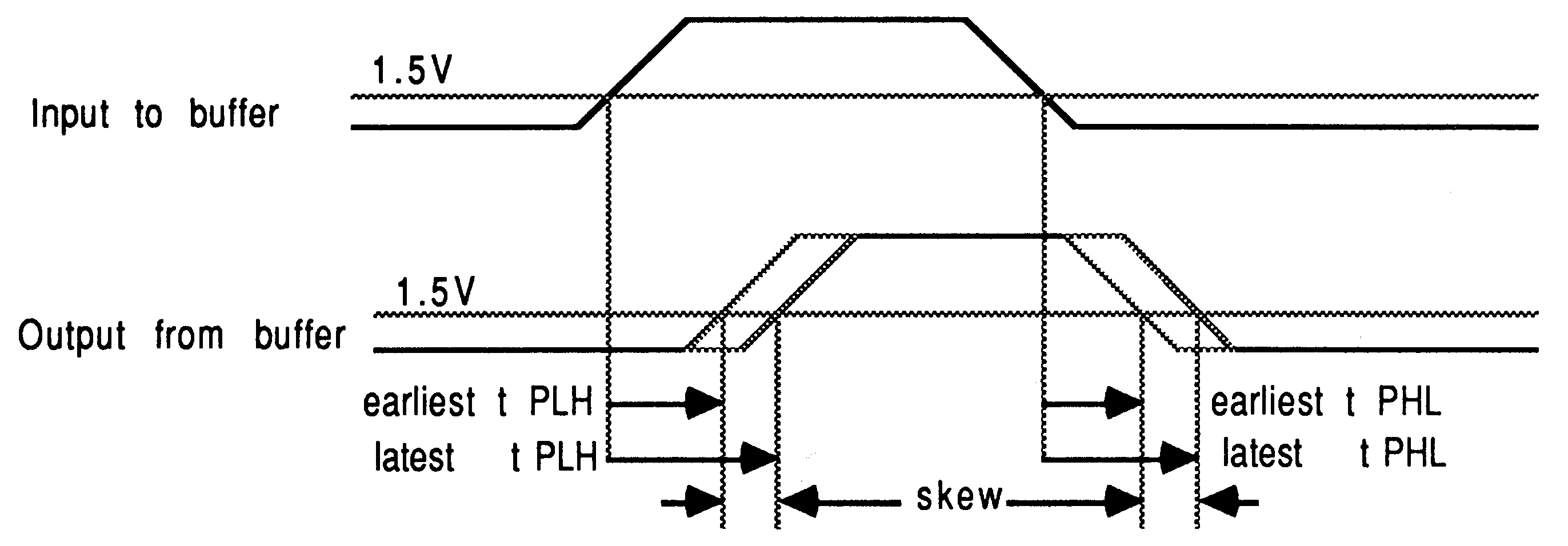
Figures 19 and 20 show some of the causes of skew. Figure 19 demonstrates how skew is introduced by buffering link signals. The skew arises as a result of the buffer exhibiting differing propagation delays for rising (tPLH) and falling (tPHL) edges, thus distorting the pulse width and reducing the sampling window. Skew of this nature can be largely eliminated by using FACT buffers which exhibit relatively little skew.
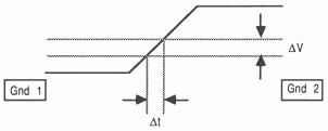
Figure 20 shows the effect of having independent grounds for each link interface. Small changes in the voltage between the separate grounds can cause ambiguous data samples. This diagram also shows the effect of a voltage caused by noise on the link data. Instantaneous voltages of this nature may also result in incorrect samples, hence the need for adequate noise control.
While the overall propagation delay of a line has no effect on the reliability of a link, there is a maximum amount of skew that the link interfaces can withstand before they fail. Table 1 shows the absolute maximum value of skew obtained experimentally that links can withstand at the three link speeds. These figures were obtained in an environment designed to be harsh by omitting a ground plane and decoupling capacitors.
| ||||||||||||||||||||||||||
This does not imply that the maximum skew figures quoted in the transputer reference manual [1] should be exceeded.
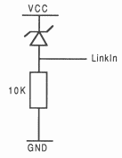
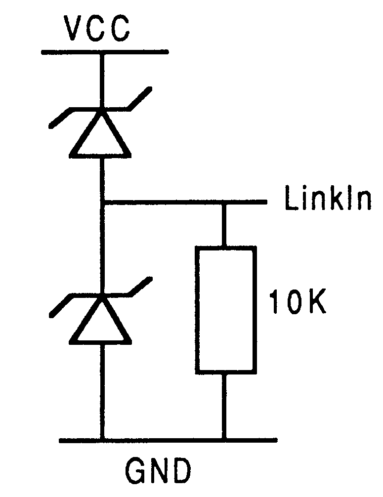
In order to protect links from electrostatic discharge (ESD) the circuit shown in figure 21 is used. The circuit is required for each LinkIn pin. The Schottky diode protects the link from ESD up to 2kV, while the resistor prevents the link input from floating high when not in use. The diode also helps to eliminate overshoot on received link signals by turning on when LinkIn rises more than about 0.4V above Vcc.
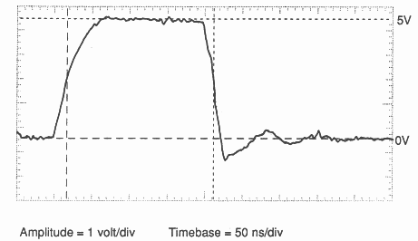
Figure 22 shows a plot of a bit received at a LinkIn. Note how the clamping effect of the diode eliminates any overshoot on the leading edge of the pulse. With the addition of another diode (figure 23) the circuit can be used to terminate a transmission line. The diodes clamp signal overshoot in both directions.
When operating over short distances, e.g. within an ITEM, standard twisted-pair link cables provide a reliable link medium at all link speeds (5, 10 and 20 Mbits/s). Over longer distances, however, reliable transmission is affected by the characteristics of the line i.e. attenuation, pulse distortion and noise susceptibility.
One method of overcoming these disadvantages is to use an optical fibre. It is not the intention of this application note to educate the reader in all aspects of optical fibres. The purpose of the note is a simple discussion of the issues that arise when engineering an INMOS link, using optical fibres.
Optical fibres have a very high bandwidth, greatly reduced attenuation and are physically very light compared with more conventional media e.g. coaxial cable.
Optical fibres exhibit no susceptibility to crosstalk or external noise.
Owing to the total electrical isolation offered by optical fibres there is no danger of ground current loops and ground noise being coupled between individual systems.
An optical fibre system is inherently difficult to tap onto. This makes it almost impossible for a third party to monitor information being transmitted on an optical fibre without being detected.
The INMOS link is an asynchronous means of sending data between transputer family devices.
Although the link was originally designed for local communication, communication over longer (> 140m) distances is best achieved by using optical fibres.
Because of the asynchronous nature of the INMOS link protocol, the propagation delay of the link does not affect reliability, it may, however, affect performance. The time delay between a transputer device sending a data packet and receiving an acknowledgement increases with the length of the link, thus decreasing effective data throughput.
The time taken to send a data packet and receive the corresponding acknowledge can be expressed by:
| Ttot = Tdp + Tap + 2lTmpd |
Where
| l | = | length of the link |
| Tdp | = | the time taken to output a data packet |
| Tap | = | the time taken to output an acknowledge |
| Tmpd | = | the propagation delay of the transmission medium per unit length |
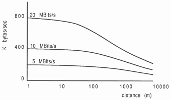
The following graph (figure 24) shows plots of maximum data throughput at the various link speeds versus length of optical fibre using the link implementation provided by a transputer family device such as the T414 or T212.
It can be seen that the difference in data throughput at different link speeds decreases with increasing length of optical fibre, the main contributing factor to the delay being the propagation delay of the medium, the constant hardware overheads becoming negligible.
It can be seen that for a medium of length approximately 500m, the effective difference in performance for the various link speeds is very much decreased. Therefore, at longer fibre lengths, there is very little advantage to be gained by operating the links at 20 MBits/s rather than, say, 5 MBits/s. This fact allows the designer to relax the constraints (especially skew) of the system.
However, the graph does not strictly apply to the link implementation provided by the T800 or T222. Increased performance is provided by such links over longer distances due to the overlapped acknowledges.
However, even with optical fibres, there is a limit placed on the maximum length of fibre owing to the skew restrictions of the INMOS link inputs [1]. This skew is caused, in the case of optical fibres, by the phenomenon known as dispersion.
There are two basic causes of dispersion, chromatic and modal. Chromatic dispersion arises from light of different wavelengths propagating at varying velocities through the fibre. Modal dispersion is caused by reflections at the interface between the core and the cladding of the fibre. This results in the reflected wave having a longer effective path length than a wave propagating directly through the fibre with no reflections.
Owing to the difference in path lengths, the optical signals will not arrive at the receiving end of the fibre at the correct moments in time, resulting in dispersion.
Different types of fibre exhibit varying dispersion characteristics, offering the optical system designer a range of price/performance tradeoffs. However, problems with dispersion will tend only to occur at much longer distances (> 1km).
The recommended maximum skew across the system is 30ns for the 5 Mbits/s linkspeed compared to the 20 Mbits/s tolerance of 3ns. A fibre used at low data rates can have a higher dispersion without affecting link reliability, owing to the increased skew tolerance.
When constructing a system, parameters such as attenuation, dispersion (modal and chromatic) and bandwidth must be considered when choosing an optical fibre. Speed of data transmission, skew tolerances and maximum length of fibre are determined by the characteristics of specific fibres and transmitter/receiver components.
For example, laser devices will cause less dispersion than light-emitting-diode type devices.
Graded index fibres will decrease modal dispersion.
Monomode fibres will largely eliminate modal dispersion.
For further information consult reference [7].
An optical fibre system consists of a transmitter, fibre and receiver. The technique of ensuring sufficient optical power is transferred through the system to drive the receiver correctly is known as flux budgeting. Each component in the system will have an associated power loss. The maximum length of any optical system can be calculated using the following equation:
| Pt − al ≥ Pr + Mp |
Where
| Pt | = | transmitter power(dBm) measured at the end of 1m of fibre |
| a | = | fibre attenuation per length(dB/km) |
| l | = | cable length(km) |
| Pr | = | minimum optical power required by the receiver |
| Mp | = | optical power margin set by user (>1dB) |
This note is intended to give the reader some idea of the method of implementing an optical fibre link.
For evaluation purposes a simple circuit was constructed. The devices to be used were required to be relatively inexpensive, simple to use and to comply with the constraints of the INMOS link engines. Of the devices considered, those manufactured by Hewlett-Packard were found to be suitable. Those used were:
| Transmitter : | HFBR 1402 |
| Receiver : | HFBR 2402 |
The transmitter is an 820nm Gallium Arsenide light-emitting-diode and the receiver is a PIN [7] photodiode with a TTL compatible output.
These devices simply plug directly into a printed circuit board, require a minimum of support circuitry and are fully TTL compatible.
The devices are fitted with the emerging industrial standard for optical fibre connectors, the SMA connector. This enables a fibre previously fitted with SMA connectors to be screwed directly onto the device, allowing simple interchanging of fibres. At present, these devices will only operate reliably at speeds up to 5 Mbits/s. It is expected that equally suitable components enabling higher data rates will be available in the not too distant future.
The major advantage of these devices is the fact that they are DC coupled i.e. there is no requirement for a steady stream of data passing between transmitter and receiver as is found in the more common AC coupled devices. AC coupled devices tend to require minimum data rates and impose restrictions on the duty cycle of data being transmitted. Devices of this nature are obviously of no use for link communication unless some method of encoding and perhaps having to send dummy packets is incorporated into the circuit, thus increasing circuit complexity. Such methods tend to move away from the idea of simple communication, provided by the link itself. For more information consult reference [8].
For our evaluation purposes the fibre used was 200 PCS (Plastic Clad Silica), a step index fibre [7]. This method of construction exhibits greater attenuation and dispersion than graded index fibres. However, this problem is offset by the ability of PCS to couple more optical power between transmitter and receiver.
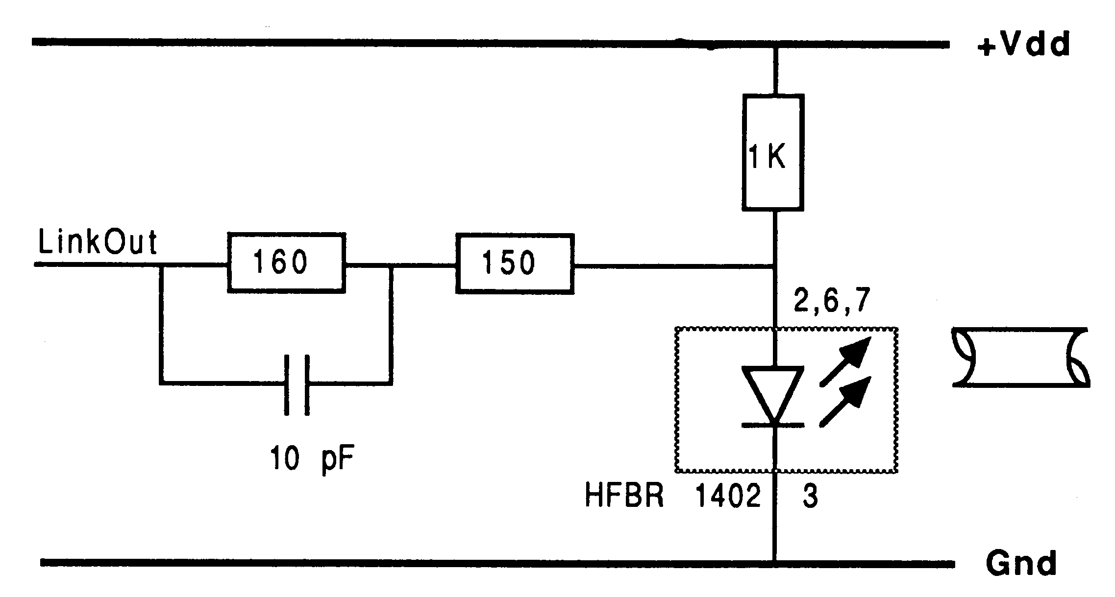
Figure 25 shows the circuit required to operate the transmitter. As can be seen, the transputer family device link output is simply directly connected to the input of the circuit. No driver circuitry is required in this case as the link output provides sufficient current to drive the optical transmitter. However for more extreme cases (e.g. longer distances or higher attenuation fibre) the LED may require more drive current in order to provide the receiver with sufficient optical power.
The component values shown are calculated from the equations given in [8] for a drive current of 25mA. The 10pF capacitor is a ’speed-up’ capacitor, intended to square the edges of the input signal.
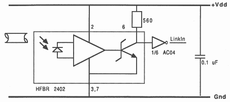
The receiver is an open-collector device, requiring a pull-up resistor. Owing to the nature of the operation of a photodiode, the incoming logic value is inverted at the output. It must be stressed that, in order to invert the receiver output signal, a FACT inverter should be used. The FACT technology provides very fast edges, with negligible skew, making FACT an ideal logic family for interfacing with INMOS links. A suitable device is the AC04 hex inverter IC. The output of the FACT buffer is connected, by methods described earlier in this note, to the input of a link.
Although optical fibres offer many advantages over conventional wire, they cannot be treated as such. Multiple fibres may be contained within a single sleeve, allowing easy installation of numerous links. In applications requiring multiple connections (e.g. an ITEM module) allowance must be made for the extra space required for the fibre bending. A typical fibre has a minimum bend radius of 2.5cm. In having multiple link connections using such devices as those supplied by Hewlett-Packard there is a problem concerning board area, as two devices are required for each link. This allows a small maximum number (approximately 3-6) of links to be realised on the edge of a double Eurocard. The devices can be placed away from a card edge. However, this increases the difficulty of repeated connection in multiple card systems.
One way of circumventing the problem of a fixed amount of optical fibre links is to use the IMS C004 [9]. This effectively allows dynamic reconfiguration of up to 32 INMOS link inputs to be connected to up to 32 outputs. This device allows the network of transputers to be reconfigured, thus allowing the optical links available to be shared between different devices on a board or in a system, giving a more efficient use of board area at slightly increased circuit complexity.
The INMOS link, by the very nature of its operation, demands a minimal delay between sender and receiver via a noise free medium. Optical fibres are able to provide such a medium and over longer distances than conventional methods.
The optical fibre electrically isolates separated sytems.
The simplicity and low cost of implementing a 5 Mbits/s INMOS link with optical fibres has been demonstrated in this note, using the devices produced by Hewlett-Packard.
It is beyond the scope of this note to discuss all aspects of optical fibre system design. For high performance systems the reader should consult reference [7].
Although links were originally designed for local communications between devices on a PCB or across a backplane, it is possible to use them over longer distances. However, some precautions must be taken to ensure reliability and integrity of data, as summarised below.
| Distance | Method | Comments |
| Up to 30cm | Direct connection | Suitable for PCBs, backplanes |
| Up to 10m | Series termination | 56Ω to match 100Ω transmission line |
| Up to 20m | FACT buffers | Minimal skew |
| Up to 30m | RS 422 | Suitable only for 5 or 10 Mbits/s |
| Good noise immunity | ||
| Over 30m | Optical fibre | Noise free, low attenuation |
| 5Mbits/s system demonstrated | ||
| Simple engineering over long distances |
[1] The Transputer Databook, INMOS Limited 1989
[2] Occam Reference Manual, INMOS Limited. Prentice Hall 1988
[3] IMS T414 Data Sheet, INMOS Limited 1986
[4] How To Control Electrical Noise, Mardiguian, M. Don White Consultants, Inc. 1983
[5] EIA Standard RS 422A, Electronic Industries Association. 1978
[6] FACT Data Book, Fairchild Camera and Instrument Corporation 1985
[7] Fiber Optics Handbook, Hewlett-Packard. 1983
[8] Optoelectronics Designer’s Catalog, Hewlett-Packard 1986