|
|
| Compiling occam into silicon _____________________________________________________________________ |
| INMOS 72-TCH-023 |
The occam language [1] allows a system to be hierarchically decomposed into a collection of concurrent processes communicating via channels. An occam program can be implemented by a single programmable microcomputer, or by a collection of programmable computers each executing an occam process. An occam process can also be implemented directly in hardware. This paper describes a compiler which translates occam programs into silicon layout.
In designing a VLSI device, it is useful to have a behavioural description of what the device does, and a hardware description of the components of the device and the way in which they are interconnected.
Hardware description languages are used in many computer-aided design systems. The hardware description of a device can be checked against the silicon layout supplied by the designer and can be used as input to simulators. The hardware description language used by INMOS allows libraries of standard checked modules to be assembled. All of these techniques combine to remove much of the risk from silicon design once the hardware description of a device has been constructed.
Behavioural description languages have been used to design sequential processors for many years. As the process of interpreting instructions in a sequential computer is (nearly) sequential, a conventional sequential programming language can be used to write the behavioural description of a processor. An advantage of using a programming language for this purpose is that the description of the device can be compiled into an efficient simulator of the device.
The behaviour of VLSI devices with many interacting components can only be expressed in a language which can express parallelism and communication. Communicating process languages are therefore beginning to be used to describe the behaviour of such devices. For example, occam has been used extensively for this purpose in the design of the INMOS transputer.
Occam has several advantages as a behavioural description language. Firstly, the concepts of concurrency and communication in occam correspond closely to the behaviour of hardware devices. Secondly, as a programming language, occam has a very efficient implementation, and this enables fast execution of a system description as a simulation. Thirdly, occam has rich formal semantics [2] which facilitate program transformation and proof, and a simple interactive transformation system has been constructed. These techniques have been used to formally establish the correctness of an occam implementation of IEEE standard 754 floating-point arithmetic [3], a task which takes too long to be performed by experimental testing. The transformation system can also be used to optimise programs and can, for example, transform certain kinds of sequential program into an equivalent parallel program, and conversely.
The problem of ensuring that the hardware description of a device indeed implements the behavioural description in occam is a significant one. One possible approach is to write a compiler to compile an occam program into a hardware description.
Occam programs are built from three primitive processes:
| v := e | assign expression e to variable v |
| c ! e | output expression e to channel c |
| c ? v | input variable v from channel c |
The primitive processes are combined to form constructs:
| SEQ | sequence |
| IF | conditional |
| PAR | parallel |
| ALT | alternative |
A construct is itself a process, and may be used as a component of another construct.
Conventional sequential programs can be expressed with variables and assignments, combined in sequential and conditional constructs. Conventional iterative programs can be written using a WHILE loop.
Concurrent programs make use of channels, inputs and outputs, combined using parallel and alternative constructs.
In hardware terms, it is useful to think of a variable as a storage register and a channel as a communication path with no storage.
Each occam channel provides a communication path between two concurrent processes. Communication is synchronised and takes place when both the inputting and the outputting process are ready. The data to be output is then copied from the outputting process to the inputting process, and both processes continue.
An alternative process may be ready to input from any one of a number of channels. In this case, the input is taken from the channel which is first used for output by another process.
The concepts of sequence and concurrency in occam are abstract, and allow a wide variety of implementations. An occam process can be implemented:
Similarly, the concept of communication is abstract, and allows a channel to be implemented in various ways:
Any of the above can be implemented using any clocking scheme, ranging from a globally synchronous system to a fully self-timed system. It should be possible to mix the implementation techniques within a system, though this requires a range of different channel implementations which operate as ’adaptors’ to provide communication between processes implemented in different ways.
Implementation of occam processes using programmable computers and transputers has been described elsewhere [4]. Implementation of processes using self-timed circuit elements is the subject of current research e.g. [5]. This paper concentrates on the compilation of a process into a tailored datapath controlled by compiled microcode. A set of concurrent processes may be compiled into a corresponding set of such machines, with each communication channel implemented by a simple synchronous connection between two machines.
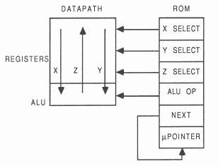
Each process is compiled into a datapath controlled by horizontal microcode. The datapath contains a set of registers connected to an arithmetic logic unit by three buses. These are called the Xbus, Ybus and Zbus. Each cycle of the machine involves transferring the contents of two selected registers via the Xbus and Ybus to the arithmetic logic unit for use as operands, and transferring the result from the logic unit back to a selected register via the Zbus.
The selection of the registers and the operation to be performed by the logic unit is determined by four components of a microinstruction held in the read-only memory (ROM). The registers in the datapath are designed so that a single microinstruction can use the same register as both an operand and as the result, but this is not essential (a compiler can easily allocate registers to avoid the need for it). The microinstruction ROM is addressed by a microinstruction pointer register.
A further ’next address’ component of each microinstruction gives the next value of the microinstruction register. The microinstruction pointer register is loaded from this field as each microinstruction is executed. The ’next address’ field can be omitted and the microinstruction pointer register replaced by an incrementer if the process to be implemented consists only of a simple loop with no conditional behaviour.
A number of other components of the microinstruction may be needed, depending on the program being compiled. These will be described below.
The compiler makes extensive use of the module library used in the INMOS transputer itself. This library contains all of the hardware modules needed to construct ALUs and registers, together with special control logic for fast multiplication, division, shifts etc. It also provides for microinstruction pointer registers, control line drivers and clock generators. The microcode ROM itself can be generated and optimised automatically from the textual form of the microinstructions. The output of the compiler is therefore:
The output can be ’input’ to the INMOS CAD system, enabling logic and circuit simulations to be performed, allowing the layout to be inspected, and ultimately enabling masks to be produced. It is, however, envisaged that the design process would be interactive, and that having inspected the result of a compilation the designer would modify the occam specification (probably using correctness preserving transformations) and try again.
Values of variables are held in registers, and expressions are evaluated as a sequence of microinstructions of the form described above.
Expressions also involve ’literal’ operands. These are derived directly from a ’literal’ component of the microinstruction. This need only be able to supply a single operand of each microinstruction, as any operation involving two literal operands can be performed by the compiler.
The compilation of:
WHILE TRUE
P |
where P is a sequence of assignments therefore proceeds as follows:
1) Identify the number of registers needed. At any point in the program, a number V of variables is in scope, and each of these must have a register allocated to it. Also, a number Tof temporary registers may be needed to hold temporary values arising during the evaluation of complex expressions. The number of registers needed for P is the largest value taken by V+T in P. This is a conventional compiling technique.
2) Identify the operations needed in the arithmetic logic unit. This depends on the expression operators used in the program being compiled. If only bit operators are used, the carry path can be omitted, and it is worthwhile only including:
if they are needed. The multiply and divide control logic require conditional selection of the next microinstruction to be executed, and this is described below.
3) Break all expressions and assignments into a sequence of operations of the form:
Z := X op Y
|
For example:
VAR a, b, result:
SEQ a := 10 b := 20 result := (a + b) - 5 |
generates microcode field definitions to control the registers, ’constants box’, and ALU, in addition to the ’next’ field. The following example is the definition of the register control field:
FIELD "Regfield" Microword[22, 23, 24, 25, 26, 27]
XbusFromR0 = #B100000 XbusFromR2 = #B010000 YbusFromR1 = #B001000 R0FromZbus = #B000100 R1FromZbus = #B000010 R2FromZbus = #B000001; |
The register R0 is used for a, R1 for b and R2 for result. R0 and R2 can supply data to the Xbus, R1 to the Ybus. All three registers can be loaded from the Zbus.
A microinstruction is constructed by combining values from each of a number of fields; for example:
LAB1: XbusFromR0 YbusFromR1
ZbusFromXbusPlusYbus R2FromZbus LAB2; |
selects R0 and R1 as the sources for the Xbus and Ybus respectively, selects the ALU operation as Plus (ZbusFromXbusPlusYbus) and selects the R2 as the destination for the result. LAB2 indicates the next microinstruction to be executed.
The microcode for the above program is:
START: XbusFrom10 ZbusFromXbus
R0FromZbus LAB0; LAB0: XbusFrom20 ZbusFromXbus R1FromZbus LAB1; LAB1: XbusFromR0 YbusFromR1 ZbusFromXbusPlusYbus R2FromZbus LAB2; LAB2: XbusFromR2 YbusFrom5 ZbusFromXbusMinusYbus R2FromZbus END; |
An example of the HDL generated is the registers a, b, result:
MODULE Registers (IN Clocks[4:1], ROMoutputs[27:22],
Zbus[31:0], OUT Xbus[31:0], Ybus[31:0]) Xreg32 R0(IN Clocks[4:1], ROMoutputs[22], ROMoutputs[25], Zbus[31:0], OUT Xbus[31:0]) Yreg32 R1(IN Clocks[4:1], ROMoutputs[24], ROMoutputs[26], Zbus[31:0], OUT Ybus[31:0]) Xreg32 R2(IN Clocks[4:1], ROMoutputs[23], ROMoutputs[27], Zbus[31:0], OUT Xbus[31:0]) END REGISTERS |
which defines the collection of the three registers and their control signals and bus connections. XReg32 is itself the name of a module which defines a 32-bit register with outputs to the Xbus; YReg32 similarly defines a register with outputs to the Ybus.
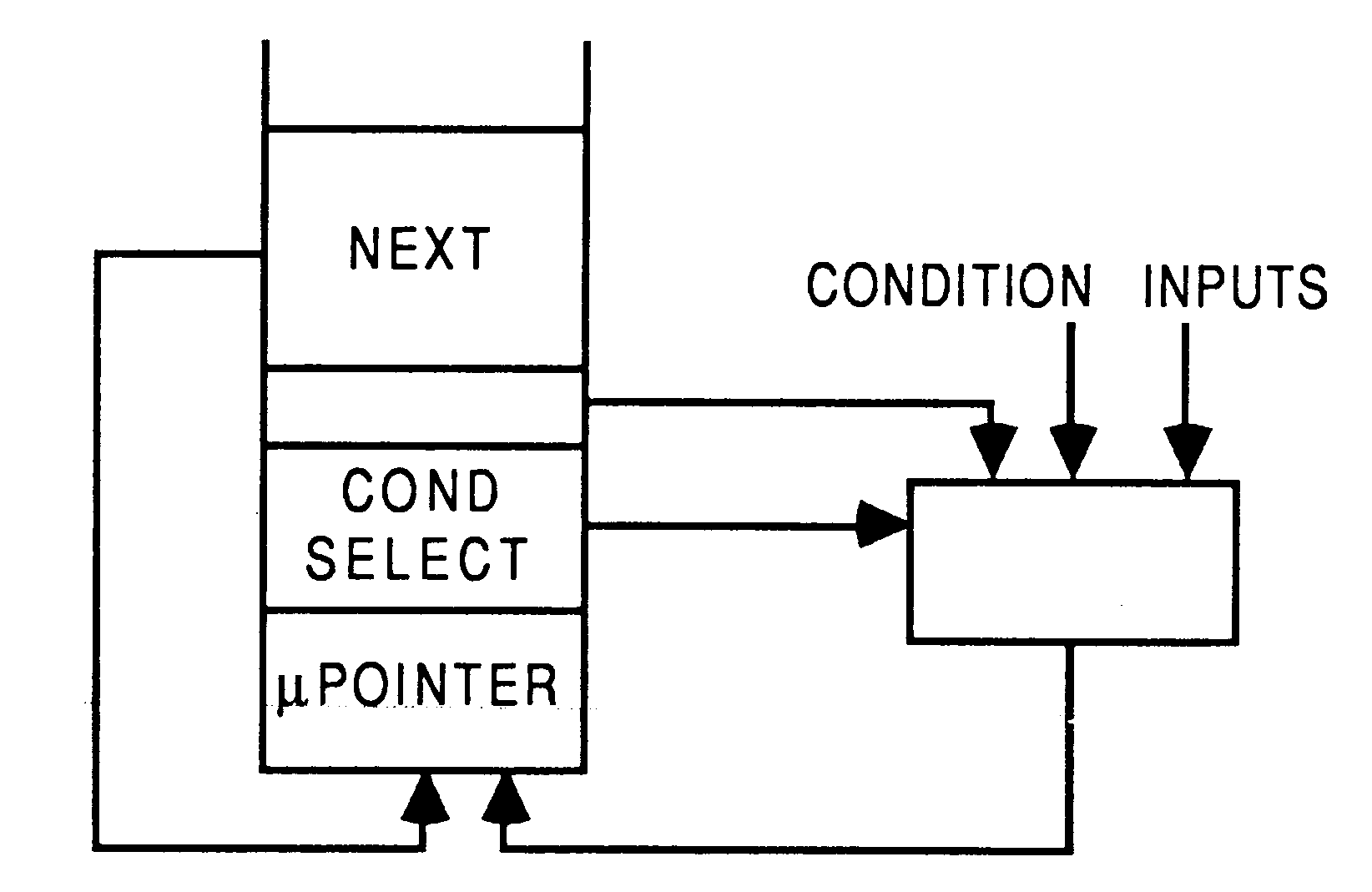
The occam IF and WHILE constructs can both be implemented by allowing the address of the next microinstruction to be determined by a selected condition.
Conditional behaviour is provided by arranging for the least significant bit of the microinstruction pointer to be loaded from a selected conditional input; the selection being made by a further microinstruction field connected to a multiplexor. To allow unconditional branching, one input from the multiplexor is derived from the least significant bit in the ’next address’ field.
An example is the following process which computes the greatest common divisor of two numbers:
VAR m, n, result:
SEQ m := 100 n := 35 WHILE (m <> n) IF (m > n) m := m - n (m < n) n := n - m TRUE SKIP result := m |
which generates the following microcode, and requires three registers for m, n and result:
START: XbusFrom100 ZbusFromXbus
R0FromZbus LAB0; LAB0: XbusFrom35 ZbusFromXbus R1FromZbus LBL0; LBL0: XbusFromR0 YbusFromR1 ZbusFromXbusMinusYbus (CondFromNotZbusEq0 -> LAB1, LBL1); LAB1: XbusFromR1 YbusFromR0 ZbusFromXbusMinusYbus (CondFromZbusGr0 -> LBL2, LAB2); LAB2: XbusFromR0 YbusFromR1 ZbusFromXbusMinusYbus R0FromZbus LBL0; LBL2: XbusFromR0 YbusFromR1 ZbusFromXbusMinusYbus (CondFromZbusGr0 -> LBL0, LAB3) LAB3: XbusFromR1 YbusFromR0 ZbusFromXbusMinusYbus R1FromZbus LBL0; LBL1: XbusFromR0 ZbusFromXbus R2FromZbus END; |
Arrays are implemented by including a random access memory. Indexing operations are provided by constructing the bitwise OR of the base address and the subscript (the base being a literal and the subscript being held in a register), eliminating the need for address arithmetic and enabling a selected component of an array to be transferred to or from a register in a single cycle. The base address of each array in the process is chosen to make this possible, and unused rows are omitted from the memory array.
Occam procedures can be implemented either by substitution of the procedure body prior to compilation or by a conventional closed procedure call.
As no recursion is permitted, the maximum depth of calling is known to the compiler, and it is possible to compile a stack of microinstruction pointer registers of the appropriate depth. Dedicated registers can be allocated for the variables in each procedure; temporaries can be shared by all procedures as occam does not contain functions..
The easiest way to implement concurrent processes is to use one processing element for each process, and the present compiler does this.
Synchronisation of input and output requires that the processor idles as the first process waits for the second. This is achieved by a microprogram polling loop.
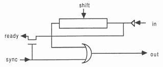
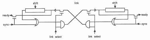
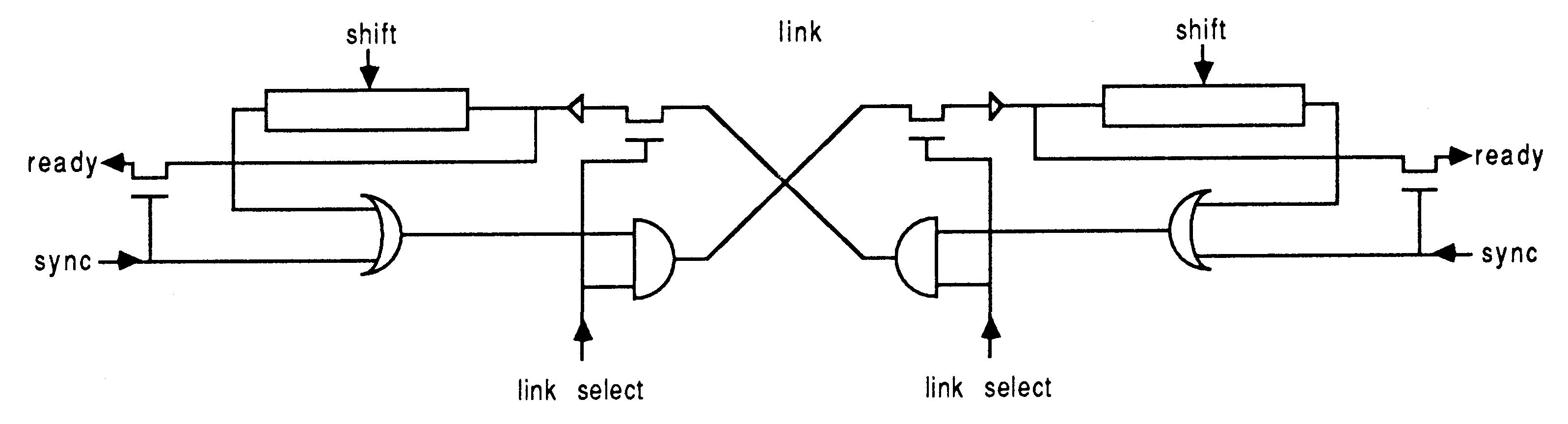
It is clearly desirable to minimise the amount of hardware associated with each channel, and to minimise the number of connections needed to implement a channel.
For any process which includes channel communication, the compiler generates a shift register, two control signals, sync and shift, and an input to the condition multiplexor, ready.
For each pair of devices which communicate, two connections are used to form a link. Each link is connected to a device as shown; only one additional control signal is needed for each link on a device; this is used to select which link is in use.
An input or output is performed by asserting the sync signal together with the appropriate link select signal, and polling the ready signal. When a ready signal is detected, this indicates that both devices are ready to communicate. At this point the process at the other end of the link will also have detected a ready signal. Both devices now release their sync signals, and clock their shift registers using the shift signals. With only the link select signals asserted, the two shift registers at either end of the channel effectively form one long cyclic shift register, so the data in the two shift registers is exchanged. After the data has been exchanged, the link select signals are released.
Clearly, this operation is completely symmetrical. Each link between two devices can be used for both input and output; it is not necessary for these to be performed concurrently as each device implements only one process.
An example of a simple process which inputs a value, adds 1, and outputs the result is:
CHAN c, d:
VAR x: SEQ c ? x d ! (x + 1) |
The microcode is as follows:
SETUP0: YbusFrom32 ZbusFromYbus T0FromZbus
SelectCh0 SYNC (CondFromReady -> TRANSFER0, SETUP0) ; TRANSFER0: XbusFromT0 YbusFroml ZbusFromXbusMinusYbus T0FromZbus SelectCh0 ShiftChan (CondFromNotZbusEq0 -> TRANSFER0, DONE0) ; DONE0: XbusFromChan ZbusFromXbus R0FromZbus LAB0 ; LAB0: XbusFromR0 YbusFrom1 ZbusFromXbusPlusYbus ChanFromZbus SETUP1 ; SETUP1: YbusFrom32 ZbusFromYbus T0FromZbus SelectCh1 SYNC (CondFromReady -> TRANSFER1, SETUP1) TRANSFER1: XbusFromT0 YbusFroml ZbusFromXbusMinusYbus T0FromZbus SelectCh1 ShiftChan (CondFromNotZbusEq0 -> TRANSFER1, END) ; |
A temporary register (T0) is introduced to count the number of bits to be transferred to or from the channel register (CHAN). The value of x is held in a further register (R0). The ALU is used to decrement the count register and test for zero at the same time that each bit is shifted through the link.
Alternative input requires that the inputting processor can poll a number of channels in turn until one is found to be ready for input. The link implementation described above can be used for this purpose; an example is shown below:
ALT
in1 ? X count := count + 1 in2 ? x count := count - 1 |
The microcode for polling the channels is:
LBL1: SelectCh0 SYNC
(CondFromReady -> TRANSFER1, LBL2) TRANSFER1: ... LBL2: SelectCh0 SYNC (CondFromReady -> TRANSFER2, LBL1) TRANSFER2: ... |
The microcode loop attempts to synchronise with each of the two links until it succeeds, in which case it continues with the input.
Prime numbers can be generated concurrently using a ’processor farm’. A program is given in [6]. It uses a controller which farms out successive numbers to an arbitrary number of primality testers. Each tester stores all of the primes up to the square root of the number to be tested; it uses these to test whether or not the number is prime, and responds to the controller accordingly.
Here we use an even simpler program. Each tester divides its new number by all numbers up to the square root of the new number. This removes the need for an array to store the prime numbers up to the square root.
This is entirely justified because we are trying to optimise the use of silicon area; the area taken for one tester with memory can be better used for many testers without. This is certainly true for generating primes up to 232.
PROC primetest(CHAN from.controller, to.controller)
DEF isprime = 0, notprime = 1: VAR maxtest, candidate, active: SEQ active := true WHILE TRUE SEQ from.controller ? maxtest; candidate IF maxtest = 0 active := FALSE maxtest <> 0 VAR nexttest: SEQ nexttest := 3 WHILE ((candidate REM nexttest) <> 0) AND (nexttest < maxtest) nexttest := nexttest + 2 IF nexttest < maxtest to.controller ! not.prime TRUE to.controller ! is.prime |
The controller is about 1.5 mm x 2.5 mm in area; each tester is about 1.2 mm x 2.3 mm. The space occupied by a controller with sixteen testers is about 50 mm2, and can easily be implemented on a single chip using a current manufacturing process. Such a chip would require very few external connections; a single link, clock and reset inputs, and power. There is a great deal of freedom in configuring the devices on the chip, as they communicate only by two-wire links. It seems likely that ’process farms’ are an effective way of organising specialised VLSI systems.
The following example is a second-order filter which filters a stream of values. It would normally be used as a component in a pipeline in which each component filter has different parameters.
PROC Filter (Chan In, Out)
VAR x, y, t1, t2, t3, z1, z2: SEQ z1 := 3 z2 := 4 WHILE TRUE SEQ in ? x t1 := x - (b2 * z2) t2 := a2 * z2 z2 := t1 - (b1 * z1) t3 := t2 + (a1 * z1) out ! t3 + (a0 * z2) in ? x t1 := x - (b2 * z1) t2 := a2 * z1 z2 := t1 - (b1 * z2) t3 := t2 + (a1 * z2) out ! t3 + (a0 * z1) |
This requires 9 registers and 93 microinstructions; the relatively large number of microinstructions arises because each multiplication requires a short sequence of microinstructions including a loop. This could be improved by providing microcode subroutines (using an additional microinstruction pointer register). Multiplication speed could also be improved (at the expense of area) by use of a parallel multiplier.
The filter occupies 3 mm2; so a pipeline of 20 filters could be fitted on a single VLSI device.
Our final example is a simple programmable processor with a (very) reduced instruction set. Despite its tiny instruction set, it provides all of the functions needed to implement a sequential occam process; in fact it is very easy to compile an occam process into the instruction set of this processor. The processor has four input and four output links, and 256 bytes of random-access memory.
PROC Processor(CHAN In0, In1, In2, In3,
CHAN Out0, Out1, Out2, Out3) VAR Iptr, Wptr: VAR Areg, Breg: VAR Instruction, Function, Operand: VAR Memory[ 256 ]: SEQ Memory[ 0 ] := Boot Iptr := 0 Operand := 0 WHILE TRUE SEQ Instruction := Memory[ Iptr ] Iptr := Iptr + 1 Function := Instruction /\ #F0 Operand := (Instruction /\ #0F) \/ Operand IF Function=Prefix Operand := Operand << 4 TRUE SEQ IF Function=Loadavar Areg := Memory[ Wptr + Operand ] Function=Loadbvar Breg := Memory[ Wptr + Operand ] Function=Loadalit Areg := Operand Function=Loadblit Breg := Operand Function=Storeavar Memory[ Wptr + Operand ] := Areg Function=Loadaind Areg := Memory[ Areg + Operand ] Function=Storebind Memory[ Areg + Operand ] := Breg Function=Jump Iptr := Iptr + Operand Function=Jumpfalse IF Areg = 0 Iptr := Iptr + Operand TRUE SKIP Function=Equalalit Areg := Areg = Operand Function=Addalit Areg := Areg + Operand Function=Adjust Wptr := Wptr + Operand Function=Call SEQ Areg := Iptr Iptr := Iptr + Operand Function=Operate IF Operand=input IF Areg=0 In0 ? Areg Areg=1 In1 ? Areg Areg=2 In2 ? Areg Areg=3 In3 ? Areg Operand=output IF Areg=1 Out0 ! Breg Areg=2 Out1 ! Breg Areg=4 Out2 ! Breg Areg=8 Out3 ! Breg Operand=Alternative ALT ((Areg /\ 1) <> 0) & In0 ? Areg Iptr := Iptr + 0 ((Areg /\ 2) <> 0) & In1 ? Areg Iptr := Iptr + 1 ((Areg /\ 4) <> 0) & In2 ? Areg Iptr := Iptr + 2 ((Areg /\ 8) <> 0) & In3 ? Areg Iptr := Iptr + 3 Operand=Greater Areg := Areg > Breg Operand=Shiftleft Areg := Areg << Breg Operand=Shiftright Areg := Areg >> Breg Operand=Xorbits Areg := Areg >< Breg Operand=Andbits Areg := Areg /\ Breg Operand=Add Areg := Areg + Breg Operand=Subtract Areg := Areg - Breg Operand=Boot SEQ In0 ? Wptr Iptr := 0 WHILE Iptr < Wptr SEQ In0 ? Memory[ Iptr ] Iptr := Iptr + 1 Iptr := 0 Operand := 0 |
On reset, the processor waits for a program to be supplied via link 0. It then loads a program, and executes it until a ’boot’ instruction is executed.
There is obviously considerable scope for better optimisation in this case; in particular it would be desirable to implement the instruction decoding ’IF’ construct with a mechanism which replaces the microinstruction pointer register with a value held in a register.
The processor requires 11 registers and has 140 microinstructions. The whole device including the memory occupies about 6.25 mm2; 10 such devices with their interconnections would take less area than a typical 32-bit microprocessor.
A communicating process language such as occam can be used to design VLSI devices, and can be compiled into silicon layout. Some parts of the design process are still performed by hand (such as the final placement of the functional blocks), but this cannot introduce errors. It is therefore possible to design concurrent VLSI systems using occam, establish that the design behaves as intended using the formal semantics of occam (or in simple cases by experimental testing of the occam program), and finally compile the occam source into correct silicon layout.
In order to simplify the construction of the compiler, many issues have been ignored. For example, the synchronous communication system is only appropriate for local communication between devices sharing a common clock. This problem can be overcome by using a different link implementation for ’long distance’ communication (for example, the link used in the transputer itself).
Expressing an application in a form which efficiently exploits silicon area involves careful consideration of the relative costs of memory, processing and communication. Concurrent algorithms which perform ’redundant’ calculations can be faster and consume less area than sequential algorithms which store values. An important use of a silicon compiler is to aid in the evaluation of ’silicon algorithms’.
[1] Occam Programming Manual, Prentice-Hall International 1984.
[2] The Laws of Occam Programming, A W Roscoe and C A R Hoare, Programming Research Group, Oxford University 1986.
[3] Formal Methods applied to a Floating Point Number System, G Barrett, Programming Research Group, Oxford University 1986.
[4] The Transputer Implementation of Occam, INMOS Ltd, Technical Note 21.
[5] Compiling Communicating Processes into delay insensitive VLSI Circuits, Alain J Martin, Journal of Distributed Computing 1986.
[6] Communicating Process Computers, INMOS Ltd, Technical Note 22.