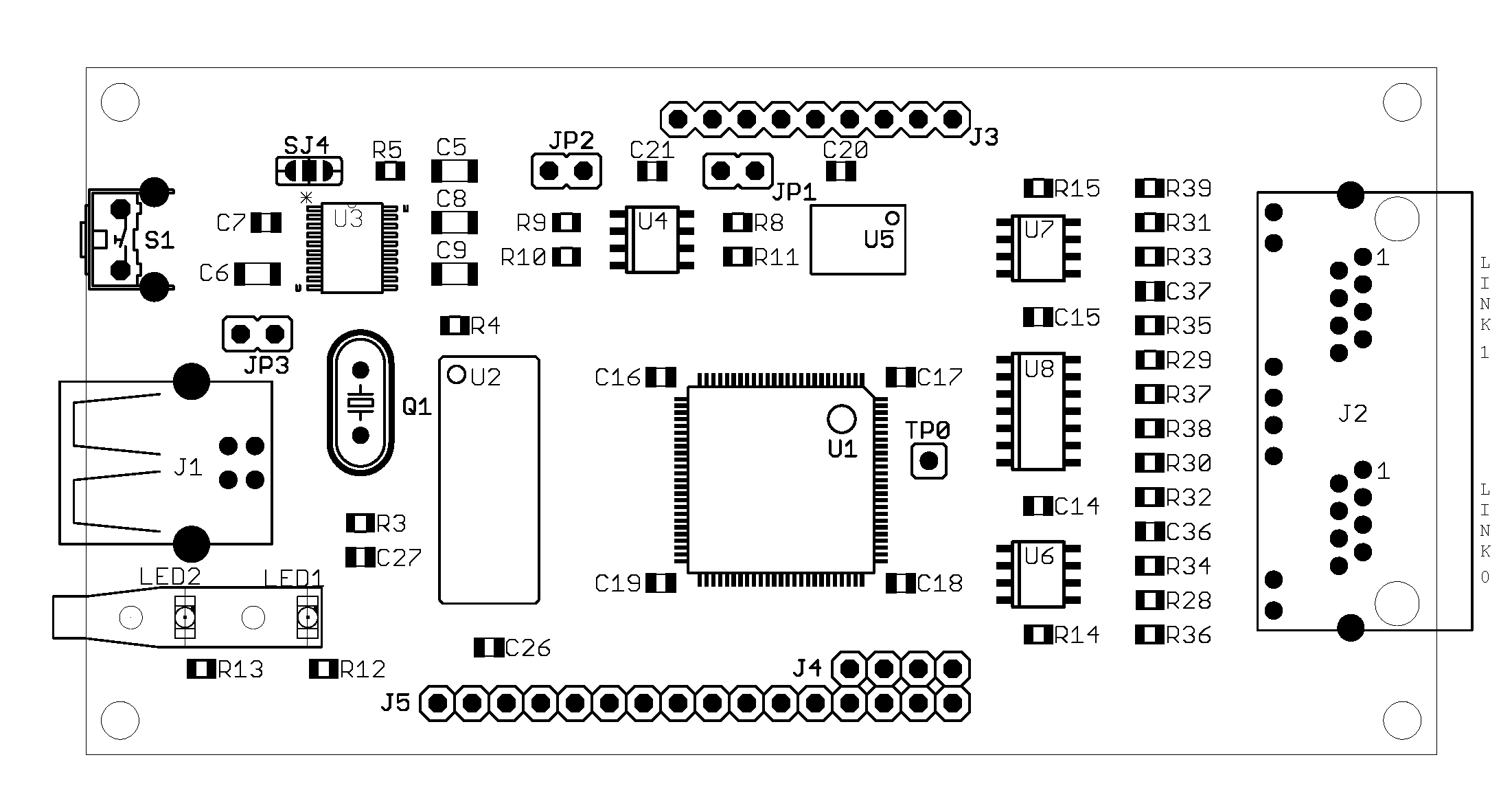
Figure 1: Top view
_____________________________________________________________________
MIKE’s Technical Note 3
April 2014
V:20250107113800
The classic INMOS transputer interfaces for connecting a transputer [1] and a PC are the two ISA-Bus interfaces B004 and B008, named after the corresponding popular PC boards. The B004 is a simple polling byte wide port interface, while the B008 expands this with interrupt and DMA capabilities.
Irrespective of the low speed (<400KB/s) and the high system impact (polling and only byte wide) is the ISA-Bus a thing of the past for PC’s build in this century.
To allow standard desktops and notebooks to interface with a transputer or a whole network of transputer the USB interface was selected. USB has many advantages which will not be listed here except one: You don’t need another wall power supply!
The LINKUSB interface device is an USB 2.0 to transputer link protocol converter. It incorporates two almost independent transputer link connectors with differential link signals and open collector control pins.
As link connector the standard RJ45 connector is used. It has the same signals and voltage levels as an Aalener link adaptor except the omitted power pin.
The link speed can be selected as 5MHz, 10MHz, 20MHz and 40MHz. Unfortunately 40MHz can only be used for testing, as there is no transputer which supports this speed. But it can be useful to check the link cable quality with a small loopback jumper.
The design is a bus powered device and the housing is a small aluminium case.
The project has its roots in 2007 after identifying the need to support the standard USB interface. By process of elimination the Cypress USB Controller CY7C68013A-56PVXC [2] was selected.
The VHDL code for the transputer link module exists from an earlier FPGA project. A Xilinx Spartan II XC2S15-5VQG100C [4] was selected due to the low complexity of the design and the 5V tolerant inputs.
The bit-stream for programming this FPGA-Type is so small that it can be downloaded from the USB Controller as a boot PROM is required for the firmware. This has also the advantage that only one PROM has to be updated and the firmware code is combined with the FPGA code.
Based on the fact that the USB controller provides four identical bulk endpoints, it was obvious to implement two distinct link interfaces.
The maximum length of an USB 2.0 cable is 5 meter. To enable longer distances between the PC and the remote transputer farm, the link interface was tied down to differential signalling. This doesn’t include the control signals: Error, Reset and Analyse. These signals are very slow and in general equipped with noise reduction circuits.
The pin assignment of the RJ45 connector allows the usage of simple standard CAT5 100baseTX crossover cables.
To utilise the RJ45 jack on both sides (UP and DOWN in INMOS naming convention) all control signals has open collector outputs and are readable. This has the advantage that the direction is only software dependent.
In 2013 there was a minor design revision.
The main changes for version 1.1 where:
To compensate the longer programming time for the FPGA a proprietary compression/decompression algorithm has been implemented. The FPGA bit-stream can be reduced from 42080 bytes to approximately 24K which is roughly the same size as the uncompressed XC2S15 bit-stream.
A special pin configuration named ”Parsytec” has been implemented which changes the analyse pin to the inverted value of the reset pin, new status LED modes has been incorporated and a few new custom commands where added.
The following thresholds should be taken as guidance levels.
The front panel consist of:
There is no difference between pressing the reset button and unplug/plug the USB cable, except that it is easier to handle.
The identification LED has two purposes: The LED is active during programming of the FPGA (about one second after power-on-reset has been released) and the identification of the device via software. If there are more than one LINKUSB devices connected to a machine, it’s much easier to identify the right module by switching on this LED, than looking for the different serial numbers on each device.
The back panel consist of a dual RJ45 jack, each with two status LEDs:
Depending on the configured mode the green LED (left) and the yellow LED (right) can be configured to show different information:
| Mode | Green | Yellow |
| Off | - | - |
| Standard | Send/Receive Data | Error or Fault |
| Data Only | Send Data | Receive Data |
| Debug | Send FIFO Empty | Receive FIFO Full |
The LED brightness for data transfers is not content dependent. Sending a long run of bytes with only 0 bits is as bright as sending bytes with all bits 1.
The Fault-State is an internal state which signals one of the following illegal receiving sequences:
To clear this condition, an explicit custom command (initialize) has to be send to the affected link.
All pins are 5V TTL compatible. Pin 1 is under the yellow LED.
Every subsystem pin has a 2.2KOhm pull-up resistor. Additionally every subsystem input pin has a simple RC low pass filter (100Ohm, 100nF) to increase the noise immunity.
RX+ has a 2.2KOhm pull-down, RX- a 2.2KOhm pull-up resistor. From RX+ and RX- there is a separate 100Ohm resistor to a common 100nF capacitor to ground for impedance matching.
The device and the transputer are not electrical isolated. This can lead to problems if only one is powered particularly over a longer time. As a consequence of this, current can flow into the unpowered device. If totem-pole drivers are involved (e.g. transputer configured as UP system and driving Reset and Analyse) this problem should kept in mind and considered. The best way to avoid this issue is to use open collector outputs for all subsystem signals.
The circuit board is a four layer 100mm x 50.8mm standard FR4 PCB. Layer 2 is the dedicated ground plane and layer 3 contains the three power areas (5V, 3.3V and 2.5V).
Besides the main actors XC2S30-5VQ100C [U1] and CY7C68014A-56PVXC [U2] there are a few other integrated circuits mounted:
The dual linear power regulator is a TPS70258 [U3] from Texas Instruments.
The serial I2C EEPROM is a 24FC512-I/SN [U4] from Microchip Technology. If the [JP1] is not present the PROM is write protected.
For the differential link signal the well-known DS89C21TM [U6,U7] from Texas Instruments is used. There is one for each link.
Finally to protect the FPGA the subsystem signals are driven by a hex buffer SN74LV07AD [U8] also from Texas Instruments.
This device has no USB logo as this module has not performed any compliance program from the USB consortium.
The VendorID is 0x16C0. The ProductID is 0x09CE.
This VendorID is shared by several people. A small range of ProductID’s has been acquired and should be unique.
A more detailed description of the endpoints can be found in the Firmware section.
The firmware is stored in the I2C EEPROM and loaded automatically into the internal RAM by the FX2LP Microcontroller.
After a basic internal setup, the first task is to program the FPGA. This code section reads the compressed bit-stream from the PROM which is then decompressed and the FPGA configured (slave parallel mode). When this has been accomplished the whole USB configuration of the FX2LP is performed which setup up the slave FIFO interface.
Finally the controller execute an endless loop and polls the subsystem status respectively handles the possible setup requests from the host controller.
Default settings:
| LinkSpeed | 20MHz |
| LedMode | Standard |
| SubSysDirection.0 | Down |
| SubSysDirection.1 | Down |
| PinConfiguration | Standard |
For speed and functional tests it’s possible to set a link into loopback mode. It is also possible to connect both links in a so called crossback mode. These connections are made internally in the FPGA.
| Nr | Type | Direction | Size | Address | Control |
| Zero | Control | Bidirectional | 64 | - | - |
| 1 | Interrupt | In | 64 | - | - |
| 2 | Bulk | Out | 512 (2x) | 0 (Link0) | FlagA (Empty) |
| 4 | Bulk | Out | 512 (2x) | 1 (Link1) | FlagB (Empty) |
| 6 | Bulk | In | 512 (2x) | 2 (Link0) | FlagC (Full) |
| 8 | Bulk | In | 512 (2x) | 3 (Link1) | FlagD (Full) |
Endpoint zero has special significance in a USB system. It is a CONTROL endpoint, and it is required by every USB device. The USB host uses special SETUP tokens to signal transfers that deal with device control; only CONTROL endpoints accept these special tokens.
This endpoint is also used to send custom commands to the device.
Endpoint 1 is an interrupt endpoint and sends unsolicited data to the host. If one or more subsystem signals changes a package with the new values is send to the host. This allows the provisioning of the subsystem signals in a way that not every request from the application (e.g. error signal polling) has to go the long way over the bus to the device.
The 4 bulk endpoints are responsible for the actual link data transfers and running in the so called Auto-In/Out mode.
Auto-In Mode allows the FPGA to stream data into a FIFO continuously, with no need for it or the firmware to packetize the data. For OUT endpoints, Auto-Out Mode allows the host to continuously fill a FIFO, with no need for the FPGA or firmware to handshake each incoming packet, arm the endpoint buffers, etc.
All custom commands are addressed to endpoint zero.
For a description of the USB SETUP Packet in FX2LP see [3] 2.3 USB Requests.
There is no data phase for the two commands VR_IDENTIFY_DEVICE and VR_SET_CONTROL_REGISTER. The information is transferred in the request value.
SETUPDAT[ 2 ]:
| 7 | 6 | 5 | 4 | 3 | 2 | 1 | 0 | |
| 0 | 0 | 0 | 0 | 0 | 0 | 0 | ? | 1 = Identification LED on |
Returns 2 bytes:
| Byte0 | LSB( BootError ) |
| Byte1 | MSB( BootError ) |
Possible results:
| = 0 | no error |
| ≠ 0 | problems in configuring the FPGA |
Returns 2 bytes:
| Byte 0: Subsystem Status Link0 |
| Byte 1: Subsystem Status Link1 |
Bit coding:
| RESET | 0x01 |
| ANALYSE | 0x02 |
| ERROR | 0x04 |
| FAULT | 0x08 |
Bit 3-7 are reserved.
SETUPDAT[ 2 ]:
| 7 | 6 | 5 | 4 | 3 | 2 | 1 | 0 | |
| 0 | 0 | 0 | L | 0 | 0 | 0 | ? | 1 = Activate reset |
| 0 | 0 | 0 | L | 0 | 0 | 1 | ? | 1 = Activate analyse |
| 0 | 0 | 0 | L | 0 | 1 | 0 | ? | 1 = Activate error |
| 0 | 0 | 0 | L | 1 | 1 | 0 | ? | 1 = Set loopback |
| 0 | 0 | 0 | L | 1 | 1 | 1 | ? | 1 = Initialize |
| 1 | 0 | 0 | 0 | 0 | 0 | 0 | ? | 1 = Set crossback |
| 1 | 0 | 1 | 0 | 0 | 0 | 0 | ? | 1 = Set pinmode to Parsytec |
| 1 | 1 | 0 | 0 | 0 | 1 | 0 | ? | 1 = Status LED Test |
| 1 | 1 | 0 | 0 | 0 | 0 | M | Status LED Mode | |
| 1 | 1 | 0 | 0 | 1 | 0 | S | Linkspeed | |
| L: | 0 = Link0, 1 = Link1 |
| M: | 00 = Off, 01 = Standard, 10 = Data Only, 11 = Debug |
| S: | 00 = 40Mhz, 01 = 20Mhz, 10 = 10Mhz, 11 = 5Mhz |
Returns 2 bytes:
Byte 0: EP2468STAT; (see [3])
Byte 1: Reserved;
SETUPDAT[ 2 ]: LSB( Address )
SETUPDAT[ 3 ]: MSB( Address )
SETUPDAT[ 4 ]: Reserved
SETUPDAT[ 5 ]: Reserved
SETUPDAT[ 6 ]: LSB( Length )
SETUPDAT[ 7 ]: MSB( Length )
The Length must be greater 0 and lower equal to 64.
IMPORTANT: It is illegal to change the serial number in any way and the programmer is liable for the adoption of the serial number in the firmware update routine.
SETUPDAT[ 2 ]: LSB( Address )
SETUPDAT[ 3 ]: MSB( Address )
SETUPDAT[ 4 ]: Reserved
SETUPDAT[ 5 ]: Reserved
SETUPDAT[ 6 ]: LSB( Length )
SETUPDAT[ 7 ]: MSB( Length )
The Length must be greater 0 and lower equal to 64.
It’s recommended to align and maximize the Length as every VR_EEPROM_WR command will generate a page write.
Returns 12 bytes which contains a 6 character Unicode text string.
The firmware update file is a binary file with a size of exact 32768 Bytes. It starts with the firmware in the EZ-USB EEPROM Boot-load Data Format [3] followed by the FPGA configuration bit-stream. Its exact start address depends on the compression rate.
Between these two sections is a special structure stored called ”MyVitalProductData”.
It contains the following information:
The structure starts with a header and one or more info blocks. The MVPD_KEY starts always at a 16 Byte boundary. Currently this is 0x1000 but may be changed in the future. To validate the structure the sum of all bytes modulo 256 must produce 0. Integer values are stored in little-endian format.
From the supplied binary files a short name, the version, the last written timestamp (in the Microsoft FILETIME format) and the CRC32 value are stored.
All version information is for reference purpose only, while the serial information is required for firmware updates.
The labels in square brackets refer to figure 1.
It is also assumed that the USB port is connected to a Windows PC where the LINKUSB driver is correct installed.
Let’s start with a fully disconnected device.
First check if there is short circuit between VBUS (5V) and GND. This can be measured at [JP3].
After the device is connected to a USB bus [J1] the green LED [LED1] should light up. This LED is powered from the 3.3V supply.
The 3.3V supply voltage can be measured at the capacitor [C8], the 2.5V at [C9].
To measure the current consumption it’s required to opening the solder bridge below the USB [J1] on the bottom side and connect an ampere meter. The nominal value is 120mA.
In the Windows Device Manager the LINKUSB Device with its Serial Number should appear.
If instead a Device with the ID USB\VID_04B4&PID_8613 shows up, maybe [JP2] is missing or the PROM [U4] is defective. It’s also possible that the PROM content has become corrupted. The last case requires a new initial programming cycle which is not feasible in the field.
After opening the Device Properties Dialog (Settings) activate the Identify Device. This operation doesn’t involve any FPGA resources.
If the blue LED [LED2] lights up the Host to USB connection is functional.
In the Device Properties Dialog (Settings) the Subsystem Status of both Link 0 and Link 1 should be inactive (off).
If all Status values are active the FPGA may be not configured successfully. Checking the BootError value may confirm this.
With an external test switch connect each subsystem signal from the RJ45 jack [J2] with GND separately and verify the level in the Device Properties Dialog (Settings).
If all tests where passed successfully the FPGA is correct initialized and the static part inside the FPGA is operational.
The next test is similar to the previous test with the external test switch except that the corresponding action to pull the signal to ground is now made with the relevant VR_SET_CONTROL_REGISTER command.
If this is too extensive opening the Device Properties Dialog (Settings) and turning on Test LED uses almost the same FPGA resources but doesn’t test the subsystem open collector drivers.
To test each link data path it is necessary to put the particular link into the loopback mode.
Every byte which has been send should be available for read back without delay. It is possible to send up to 1024 Bytes in one write operation if there is also a subsequent read operation with a sufficient buffer.
In case of problems visually check the 80MHz oscillator [U5].
To extend this test and involve the line driver/receiver it is necessary to switch off the loopback mode and use an external loopback plug like the COMPAQ 317463-001.
When using a crossover cable it is also recommended to re-check the subsystem signals. If activating the Reset on one side both Subsystem Status signals should be on. Continuity check of the cable is also recommended.
As the transputer link protocol is stream oriented and the USB bulk transfer is block oriented it is necessary to commit partial filled blocks. This will be made after the last received data byte and an additional wait time of approximately sixteen bit time segments.
It is not guaranteed that the receive block length matches the send block length.
This device buffers and acknowledges incoming link data as long as buffer space is available. This behaviour may be interpreted by the other communication partner as a ready to go sign which is maybe not desired.