|
|
| IMS B007 A transputer based graphics board _____________________________________________________________________ |
| Ray McConnell April 1987 |
This application note describes the implementation of a high performance, medium resolution graphics hardware system based around the IMS T414 processor.
In all raster scan video display systems the displayed picture is constructed from a matrix of coloured dots. The dots RED, GREEN and BLUE are made sufficiently small and physically close that the eye can only perceive them as one mixed colour. Each phosphor colour is made to glow by firing a different electron beam at it. The intensity of the beam controls the brightness of the dot, so by varying each beam individually a large set of colours can be produced. The intensity of each beam is controlled by an analogue voltage varying in the range from 0 to 1.0V. The beams are made to scan the display so fast that the eye perceives a continuous picture.
Raster scan graphics machines group these dots into well defined areas called pixels, and these pixels can be changed under program control. The purpose of the graphics hardware is to retrieve this pixel information from store, change the digital representation of that pixel into the three analogue control voltages and superimpose synchronising pulses onto one of these (usually green). The hardware must do this continuously for the whole display period, which is at least 50 times a second. It must always be able to display the contents of each pixel with no interruptions, to prevent the loss of synchronisation with the display monitor.
The display hardware must also arbitrate between video display update and with the transputers access to the pixel data.
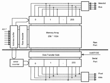
Recent developments in dynamic RAM design have produced the dual port or video RAM. This is essentially is a standard dynamic RAM with an extra serial access port, that can operate totally asynchronously with the processor’s random access port.
With reference to the above diagram, the bulk of the memory array has two access ports, the random access port and the serial access port. The RAM port is a standard dynamic RAM interface. The serial or video port is sequential read only, and needs to be reloaded once every 256 nibble wide reads. When all the data has been read, it needs to be reloaded; if this port is not reloaded it will simply wrap around and start to repeat data already used.
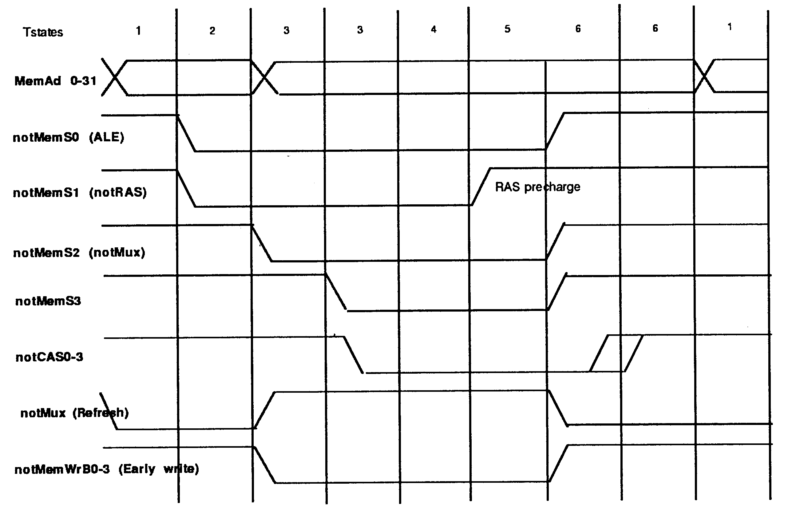
Because the video port shares the bulk memory array with the RAM port, the video hardware needs to prevent the processor from accessing the RAM during an update. To do this the video hardware must halt the transputer and steal a memory cycle. The transputer is halted by asserting MemReq and waiting for the transputer to reply with the assertion of MemGranted. This tristates the MemAD bus and deasserts the control strobes. A control pin on the video RAM is then asserted (notDT/OE), and a conventional address multiplexed access executed by the video logic. The selected row is placed in the video port, and the column address placed into the serial counter. The transputer is then allowed to continue by deasserting MemReq.
Once the serial port is loaded it can output data sequentially totally asynchronously with the RAM port, starting with data addressed by the serial counter. The counter is incremented every video port clock rising edge.
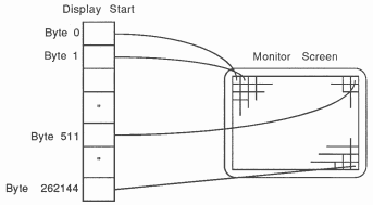
Ideally, from the programmers point of view, the video frame store should have a one to one correspondence to the displayed data. This allows the programmer to manage the displayed data in a short learning time and considerably simplifies any graphics algorithm used (thereby generally speeding things up).
Bearing this in mind and as a compromise between speed, simplicity and number of displayable colours, 8 bit pixels are used, mapped onto 512 rows of 512 pixels. As in the diagram above, each pixel maps to a byte addressed in the frame store. Each successive byte corresponds to a successive pixel on the display. This allows a two dimensional vector of bytes to map directly onto the display, starting with DisplayByte[0,0] at the top left and finishing with DisplayByte[511,511] at the bottom right.
Using this data representation, transputer block moves within the video store become meaningful as fast display management primitives, thus allowing very fast manipulation of any area of the display. Also the transputer’s autonomous links can slice data into the display allowing the frame store data to be derived from a network of transputers. The block move instructions allow four bytes to be transferred every two memory interface cycles (in this case eight processor cycles of 66ns) or approximately 7.5 MBytes/second. In real terms, this allows 30 complete 1/4 megabyte display block moves per second. With all links running at full speed, frames generated on an array of transputers can be displayed at 8 frames per second.
With this powerful feature, for example, a transputer graphics board could become a graphics command interpreter, receiving commands via links (fast graphics primitives residing in internal RAM), or an intelligent frame store connected to large computing engines built from arrays of transputers, which pump data straight to the frame store via the four INMOS links. Using a mixture of both techniques described above, fast animation based on graphic templates with block moves has produced quite stunning displays.
To allow double buffering techniques to be used (filling one buffer while using the other), the board was designed with two separate display storage areas. Each display consists of eight 64K by 4 video RAMS, giving 1/4 megabyte of store per display. In addition, a further 1/2 megabyte of store is available for general purpose program and workspace (perhaps a graphic template store). The board therefore has a total of one megabyte external storage plus 2 kilobytes of high speed internal transputer RAM.
The design of the board is split into three sections - the processor random access read write port, the video serial port and a sophisticated reset scheme - to allow systems to be plugged together.
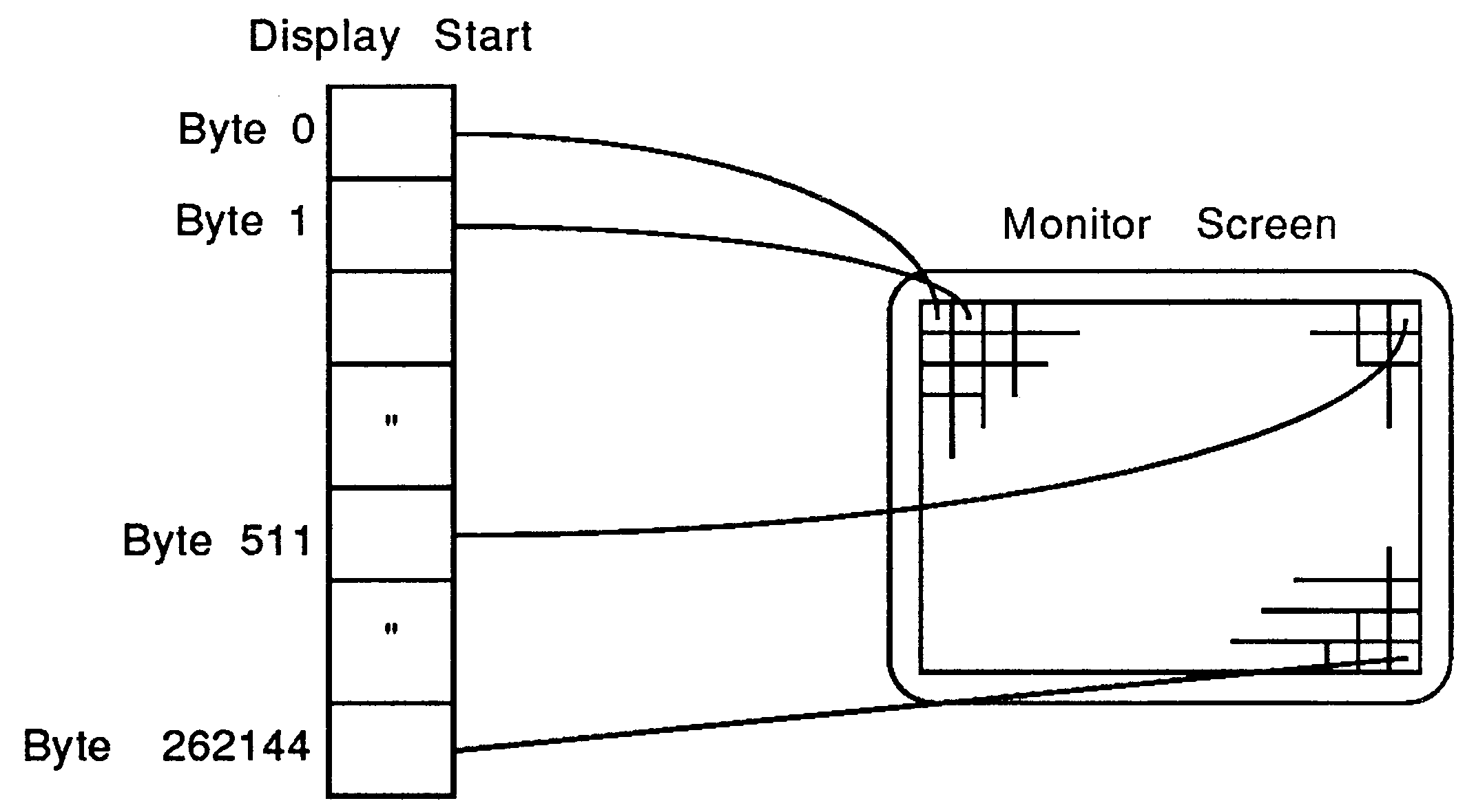
The T414’s memory interface is configured from a PAL (AMD PAL 22V10). As it is necessary to latch addresses off chip, some external logic is necessary.
Generally for dynamic RAMS three timing strobes are needed,
row address strobe address multiplex strobe column address strobe
In this design, the configurable strobes notMemS1 to notMemS3 are used to generate the above strobes. Decoding is done with a PAL (AMD 22V10) and is done using the CAS strobes.
As the above diagram shows, this design uses the high order 8 bits (A10 to A17) as the row address and the low order 8 bits (A2 to A9) as column address. This non standard technique has the effect of mapping consecutive addresses in the video ram onto the same address row. Thus when the row is loaded into the dual port, successively addressed data will be presented to the serial output, producing the effect of horizontally mapped data from left to right across the display.
Unfortunately this has the side effect of complicating the dynamic ram refresh, as refresh addresses supplied by the transputer’s memory interface are mapped onto the low order addresses. To solve this problem the high order 8 bit address is swapped with the low 8 bit address at refresh. This is done using three exclusive OR gates.
Since the design uses four banks of 64k by 4 dynamic RAMS, a one of four selector is necessary for RAM decoding. This is done by the PAL. Address bits 18, 19 and 31 are latched externally and input to the PAL, decoding is achieved by providing a CAS strobe timed from notMemS2 and all other banks are harmlessly refreshed.
One further complication arises during the dual port re-load when the bus is requested by pulling MemReq high. When MemGranted goes high all strobes go high and the address/data bus goes tristate. This causes a problem in that the address multiplex strobe is derived from notMemS2 and the Row address buffer output enable is an inversion of notMemS2, and is therefore active. To prevent this notMemS2 is gated with MemGranted.
The graphics board peripherals are also decoded in the PAL, and are selected when A31 is low, using A18 and A19.
The board has been designed to drive the memory interface in four processor cycles as can be seen in the timing diagram shown.
The video port consists primarily of four groups of logic,
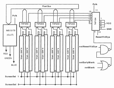
the serial outputs of the video rams with pixel multiplexer and control logic video timing and address generator the colour look up table a group of memory mapped control bits that provide a reset to the video logic and a control bit to select which screen is presently being displayed.
Two displays are resident, allowing double buffered animation techniques to be used. Each display consists of eight 64k by 4 video rams, arranged in pairs to give four byte wide banks. The transputer views these banks simply as byte[0..3]. The display logic multiplexes between these banks to provide a single byte wide pixel bus, allowing consecutive bytes to be displayed as consecutive pixels.
The serial data outputs of the video RAMS from both displays are connected to the inputs of a group of four octal buffers (only one set of display serial outputs are enabled at any one time). The outputs of the octal buffers are all joined to the 8 bit pixel bus. The tristate control of each of these buffers is controlled using a travelling zero bit in a field of four bits. This is achieved using a pre-loadable shift register (74F194), which is clocked directly by the pixel clock (Pclk), and the last output tied to the serial input. Each output enable strobe is also connected to the serial clock of each respective byte of the video ram, clocking the ram as it is deselected (the serial port is clocked on the rising edge of the clock). This allows the pixel clock to exceed the permissible individual clocking speed of the video ram by a factor of four.
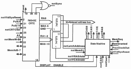
The control of the video port is achieved using a simple and inexpensive CRTC (Cathode Ray Tube Controller) chip, namely the Rockwell 6545E CRTC (a Motorola 6845 superset) and some additional logic components. This chip is primarily designed as a character display generator for terminals and home computers. It interfaces to the transputer’s memory interface with the aid of a wait state generator. It can be programmed to drive various ranges of monitors with or without interlace. The logic also allows this device to cause transputer events (hardware rescheduling of a process), allowing an occam process to synchronise with an external hardware event, namely frame flyback. This is achieved by latching the cursor output to EventReq, and resetting this with EventAck event handshake. The cursor is programmed to be a simple underline and to occur at the last character position in the display.
When a line is to be displayed it must be loaded into the video port. The address for the line to be displayed and the start location of that line is supplied by the CRTC. The CRTC in its normal working mode continually supplies addresses of character positions and line of character during the line scan.
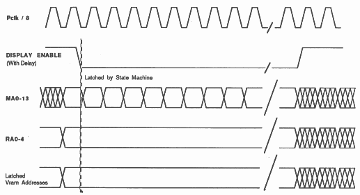
The first address that the CRTC outputs at the beginning of the line is latched, and is used to point to the line and starting point of the data in the video RAM. Fifteen addresses are latched, allowing a coarse pan and scroll (resolution of 8 pixels in X and Y). A state machine built from discrete logic provides the timing for the video ram row-column address multiplexing, and synchronisation with the processor’s MemGranted. This state machine is triggered using the DISPLAY ENABLE output of the CRTC as it comes out of line blanking, and is clocked by ProcClockOut/2.
The DISPLAY ENABLE output of the CRTC is also used as an input to a delay stage clocked by Pclk/8 (serial loaded shift register 74F164). This provides a timing window for the dual port update before the display is to commence. The output of this delay stage is the input into yet another delay stage clocked by Pclk/4 (serial loaded shift register 74F1 64). This provides the timing necessary to clock the video port just once to remove last pixel data stored in the output stage of the video ram after it has been loaded. Four Pclk periods later the pixel multiplexer is allowed to run, and the IMS G170’s notBLANK input is then taken out of blanking, and the display commences. The multiplexer then runs until the end of that displayed line, when the CRTC delayed blanking strobe stops the multiplexer and asserts notBLANK, terminating the display.
The video timing synchronisation is provided by the CRTC, by gating the VSYNC and HSYNC together into the notSYNC input of the G170.
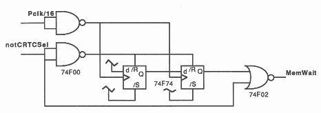
The CRTC’s processor interface needs to be clocked. This clock is provided by Pclk/16. The interface has been designed such that when the notCRTCSel select strobe from the PAL goes low, the wait pin is asserted on the transputer until at least one CRTC clock period has elapsed.
The CRTC itself provides a status register which includes information about the display frame flyback. The transputer can synchronise with frame flyback by polling this register.
The video hardware need only take one video port update cycle in more than a thousand processor memory cycles. This is also further reduced because video RAM updates are not needed during frame flyback. This gives the processor more than 99.9 percent access to the display store whilst the video port is being fully updated.
The pixel bus connects directly to the pixel input of the IMS G170. This is the INMOS high speed colour look up table which provides the digital to analogue conversion necessary to drive the standard 75 Ohm RGB inputs of colour monitors. The pixel data clocked into the G170 is used to address one of 256 locations of an 18 bit wide table. Each entry in the table has three 6 bit colour intensities, one for each primary colour. This allows more than a quarter million possible permutations of colours of which 256 are displayable at any one time.
An 8 bit addressable resetable write only register (74F259) is used as the memory mapped control bit for display select (screen flip), and video system reset. All the registers in this device are set to zero at reset. The screen flip bit is inverted, and one of the senses of this control bit is connected to the tristate output control of the display serial outputs. This ensures that both displays are not active at the same time, and one is always active (note that the screen flip needs to be synchronised to frame flyback, because as the screen is flipped data on the serial outputs are temporarily undefined and may cause noise on the display). One of the other bits of this register is used to reset the whole of the video system. Because this 8 bit register is reset at processor reset time, the display is blanked until the video system reset is set by software.
The IMS B007 shows that a high performance graphics board can be built using a transputer purely as a drawing engine. Programmed in occam it becomes both highly flexible and very fast, retaining the necessary simplicity and processor bus bandwidth achievable using dual ported rams. But where this board really stands out is the use of high speed communication links with other transputers, enabling highly concurrent, infinitely large arrays of transputers to perform the very heavy computational tasks of many graphic algorithms.