|
|
| A transputer based
distributed graphics display
_____________________________________________________________________ |
| INMOS Limited 72-TCH-046 |
This technical note examines a frame store distribution technique using the IMS T800 for high performance computer graphics systems.
In the beginning there is a brief introduction to some of the techniques and terminology used in typical graphic systems including comments on system implementation and processing implications.
Following this, section three provides an overview of parallel graphics systems and frame store distribution. There are also brief descriptions of the transputer, specifically the IMS T800 architecture, the occam language and transputer module architecture. Following this there is an introduction to the two TRAMs used to implement the distributed graphics system.
The next two sections describe the graphics TRAMs in detail, and how the distribution methods are implemented.
Finally some example system configurations are described using the graphics TRAMs and some performance implications of the configurations.
In the early days of computing, user interaction with computers usually consisted of a teletype machine with a built in keyboard. This was costly in terms of maintaining the mechanics and producing reams of partially used paper. It wasn’t long before electronic displays began to be commonly used. The first displays were essentially glass teletypes, providing the user with an electronic alphanumeric display. The visual display was constructed from a two dimensional array of dots called pixels. Each pixel had one colour and could be illuminated individually - either on or off, hence the name monochrome (monochromatic) display. From this any character could be represented provided it was constructed from a small array of dots that fitted into one character matrix size on the screen. Since then these displays have become more sophisticated, having large numbers of displayable colours and higher numbers of unique displayable dots per square unit of the screen surface.
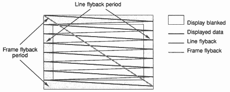
Most electronic displays consist of an evacuated sealed glass tube, with a coating on the inside surface of the display screen. A beam of electrons are fired onto the coating, which makes it glow, producing a small spot of light. Because the beam is moving charge, it can be deflected using either electrostatic or magnetic fields. Its intensity can also be controlled, changing the brightness of the spot. This allows the path of the spot and its brightness to be controlled by electronic circuitry (see figure 1).
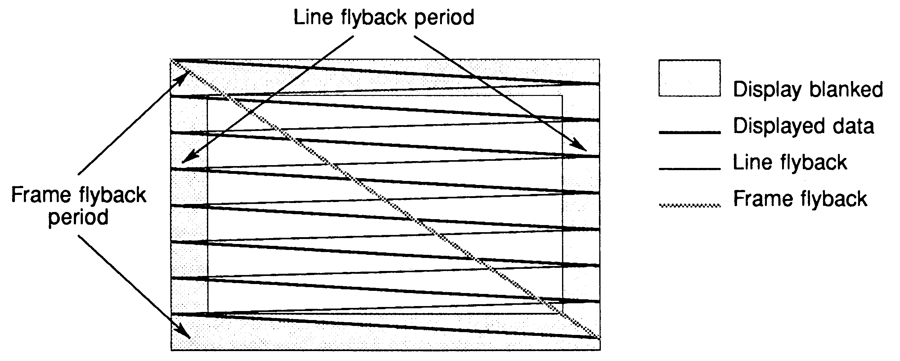
These circuits are designed to make the beam scan in a series of horizontal sweeps, left to right across the display. When the beam reaches the end of the line, its brightness will be switched off (blanked) and it will fly back at high speed to the start of the next line, slightly below the previous line. This is known as line flyback (see figure 2). This scanning will continue until the entire display has been scanned. When the beam reaches the end of the last line it will be blanked and will fly back at high speed to the top of the display. This is known as frame flyback (see figure 1). This happens so fast that the human eye cannot see the spot, and the lines are so close together that they are not individually perceivable at normal viewing distances. A small spot of light can produce a complete frame so fast that it can be animated without being perceived as individual frames. This is a similar technique to that of the film industry, where multiple still frames give the illusion of a moving picture.
Some systems use a technique known as interlace. Each frame of a scene is split into two fields. Each field contains every other line of the complete frame. So, one field contains all the odd numbered lines and the other all the even lines. This technique allows each field to be displayed for the same period as a complete frame, without causing much of a flickering effect. This halves the rate of data that needs to be displayed, reducing the necessary speed of the electronics. Television systems use this technique to reduce the bandwidth of the transmitted signal.
The circuitry controlling the horizontal and vertical scanning frequencies of the beam and the brightness of the spot can be controlled using an input control signal. This control signal is continuously variable in the range of 0 to 1 Volt. The brightness of the spot is represented by the input signal voltage level in the range 0.3 to 1 Volt. Synchronisation pulses (pulses that control the frequency of the scanning spot) are represented by the control input signal voltage level in the range 0 to 0.3 Volt (see figure 2). The synchronisation pulses are superimposed onto this signal by the graphics hardware, so that the display scanning circuitry will scan in lockstep to the scanning of the frame store. This ensures that the data representing a particular pixel on the display will always be at the same place on the screen (see figure 2).
These control signals have characteristics which have defined standards (such as the RS170 video standard) and therefore standard displays, called monitors, can be used. These monitors usually come in ranges classified by the screen dot size and the overall size of the display. It is these two factors which define the range of scanning frequencies that the monitor is designed to lock onto.
The analogue control signal is derived from a digital source. It is the job of the graphics hardware to scan and retrieve digital video data from a frame store (a digital representation of the display screen) and convert it into the analogue control signal outlined above.
There are generally two methods of implementing a frame store. These are:
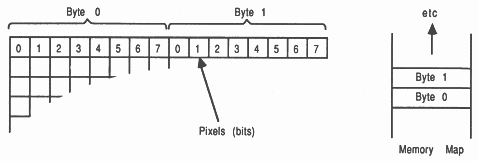
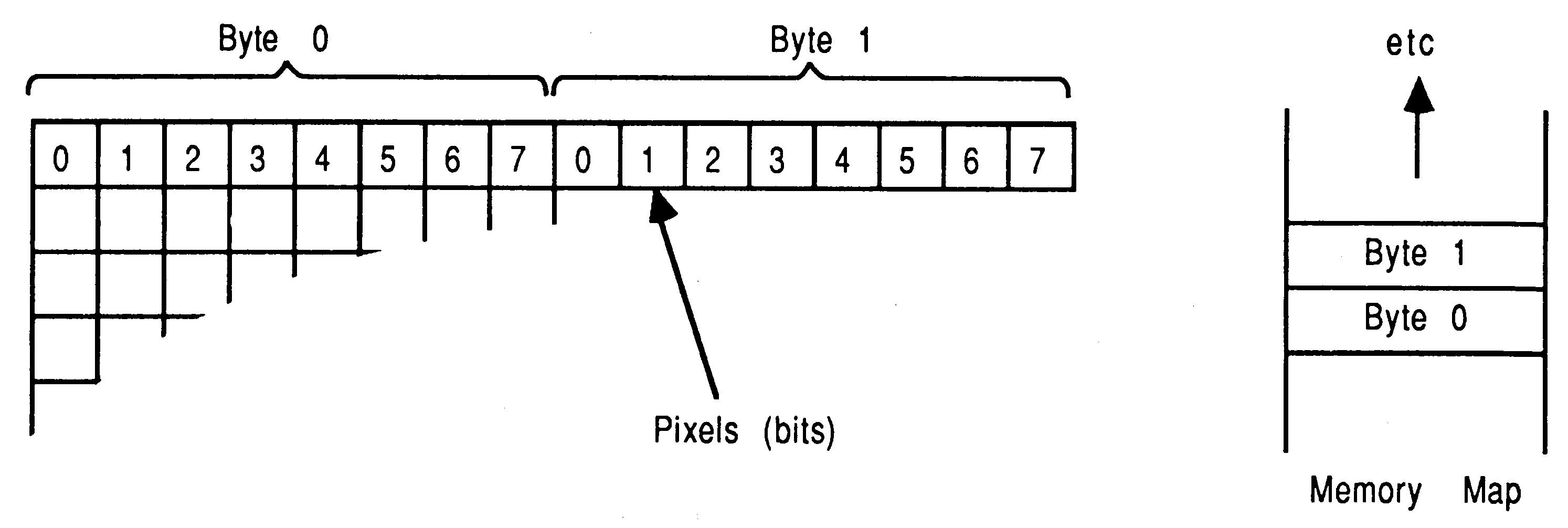
Bitmapped pixels: Data is stored (see figure 3) so that a single bit from each word of a processors store will illuminate a pixel either on or off. The method for storing the data in this way has become known as a bitplane. Monochromatic displays use a single bitplane as a frame store.
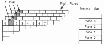
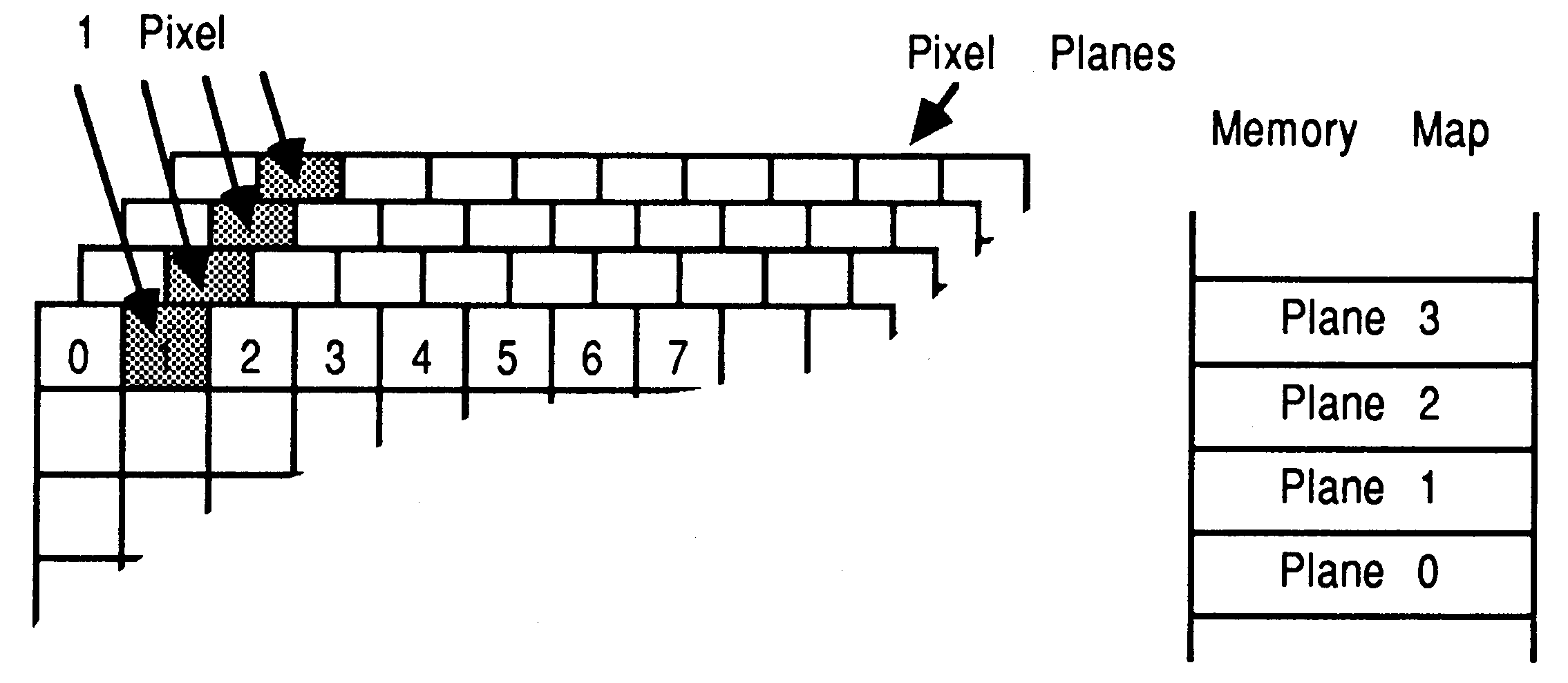
Once monochrome bitplanes were in common use, it became necessary to add colour. The extra colours are the result of adding more bitplanes and more pixels are the result of having larger bitmaps (see figure 4).
Notice that an individual pixels data is spread to several locations in store, so that an update will require several accesses to store. This allows more planes to be added to a system by increasing the amount of ram, of course the hardware must be in place to take advantage of the extra colours available.
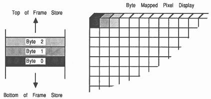
Packed pixels: Data is stored so that each pixel is located at a single address in store. This provides an efficient memory access utilisation at the cost of fixed numbers of colours per pixel.
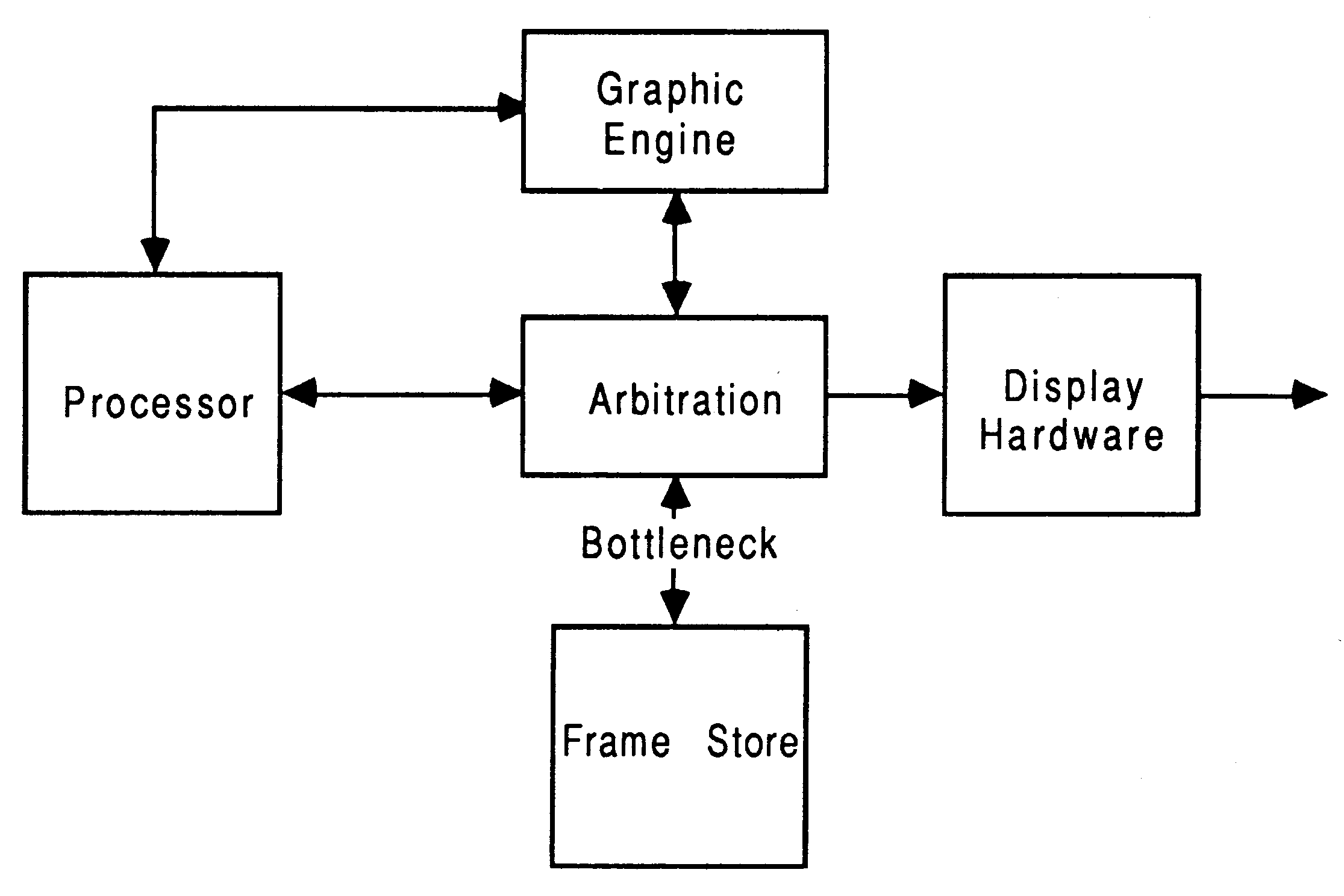
Any frame store implementation must be scanned by hardware continuously so that the pixel information can be encoded onto the analogue control signal. Also, the frame store must be available for modification by the processor. The hardware must therefore arbitrate the frame store access between the display scanning and processing (see figure 7).
Colour monitors use three different colour sub-pixels (as close to the three primary colours, red, green and blue, as possible) that can be illuminated separately. For this, three separate control signals, which vary the brightness of each colour, are necessary.
To produce these colour signals, the digital data is separated into the three colour components red, green and blue. Each is fed into a separate digital to analogue converter (DAC). The analogue signal now consists of the three separate signals representing the primary colours. By varying the digital input to these DACs the voltage levels of each these signals can be changed producing a large number of possible colours on the monitor. This can be extended so that digital pixel data can represent an address in a table which has been preloaded with various colour values for each output DAC (see figure 6).
This intermediate Colour lookup table (CLUT) can increase the total number of possible displayable colours. This is because the table width is not related to the addressable entries to the table (see figure 6). Each entry can output data to each DAC, presenting more bits to all three DACs than the input pixel data contains. Only a small number of the total displayable colours can be displayed at any one time though (the number of unique addressable entries to the table).
For example (see figure 6), the colour table may contain 256 entries, each entry is 18 bits wide, presenting 6 bits of colour value to each DAC. This gives 262144 (218) possible colour values. Any combination of these colours is allowed since the table is preloadable, but only 256 colours are displayable at any one time.
In many graphics systems, there are aspects of the design where system performance is reduced, such as in a multiple bitplane addressing (see section 2.3). Many systems become special purpose to overcome these performance problems and thereby increase the cost of the system by using custom built hardware and reducing flexibility. The following are typical areas where these problems can arise:
Pixel addressing: Each pixel may not have a unique address, i.e. when using multiple bit planes. Single bits in many locations in the frame store represent a single pixel, requiring accesses to many locations to change this pixel value. General purpose processors do not usually have the ability to manipulate data addressed in this way. Special high speed graphic processors with hardware engines need to be placed between the general purpose processor and the frame store to map pixel data into the frame store (see figure 7). These processors come in a range of configurations, ranging from full blown processors with large instruction sets, to a collection of engines designed for highly specific purposes.
Frame store access conflicts: The processor must perform drawing tasks into the frame store when the display scanning hardware is not using the frame store. This can consume processor performance because any drawing into the frame store is restricted due to the sheer amount of data that has to be shuffled out of the frame store by the display scanning hardware. This is especially so in high resolution systems. This is referred to as the frame store bottleneck (see figure 7). Consider a 512 by 512 by 8 bit pixel display. If we assume that a 32 bit read from the frame store takes 200 × 10−9 s, and the store is scanned 50 times a second (20 × 10−3 s). Then to read all the data will take 65536 reads and will take 13.1 × 10⁻³ s. This leaves the processor (20 × (13.1 × 10−3) = 6.9 × 10⁻³ s. to update the display. This leaves only 34% of the total frame store bandwidth for the processor to do anything useful.
Doubling the horizontal and vertical resolution (R) quadruples the frame store data (proportional to R2). Also, doubling the number of colours (C) will increase frame store access bandwidth. It follows that the processors access to the frame store is proportional to a CR2 law. This is doubled when we consider that the scanning hardware needs to read all this data as well. This can somewhat be relieved by using several banks of ram and using a ping-pong mechanism to switch the busses between the processor and display hardware. This is only useful in animation systems where each frame has to be completely redrawn and therefore becomes somewhat special purpose.
Compute performance: Consider animating a graphic image which consists of 12,000 points (where FLOPs means ’Floating Point Operations’).
| Operation | Units | |
| Rotate, translate, scale | 300 | KFLOPs |
| Clip (display viewable surfaces) | 72 | KFLOPs |
| Converting to screen coordinates | 130 | KFLOPs |
| Shading | 360 | KFLOPs |
| Interpolation (rounding flat surfaces) | 300 | KFLOPs |
| The approximate total is: | 1.2 | MFLOPs |
Assuming 25 frames a second, the grand total becomes 30 million FLOPs per second. This level of performance is well beyond single processor performance, indeed just shuffling the data around is beyond memory bus bandwidths of many processors.
From the above brief discussion, several requirements arise for a general purpose graphics system can satisfy the needs described:
Compute performance: Any required compute performance desired for any given application.
Drawing performance: Any required drawing performance into the frame store for a given application.
Display access: The display scanning must have separate access to the frame store to remove the conflict between the processor and the display scanning hardware.
Display resolution and colour depth: Any required display resolutions and colour depth (bits per colour).
Display drivers: Any required display output (to follow above). For instance, very high speed device technology may be necessary for a very high resolution display.
This technical note will describe a transputer based, distributed graphics system which resolves the problems outlined above.
In the previous section (section 2.6), several aspects of a graphics system were discussed.
To provide any desired processing performance requires that the processing task is divided into smaller subtasks and as many processors that are necessary to provide the appropriate performance must be used. This allows a system to be built to achieve any drawing bandwidth, with any compute performance. The problem is now one of distribution and how this is implemented.
Here are some methods for distributing processing tasks:
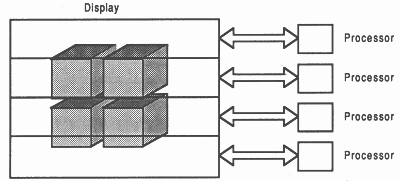
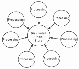
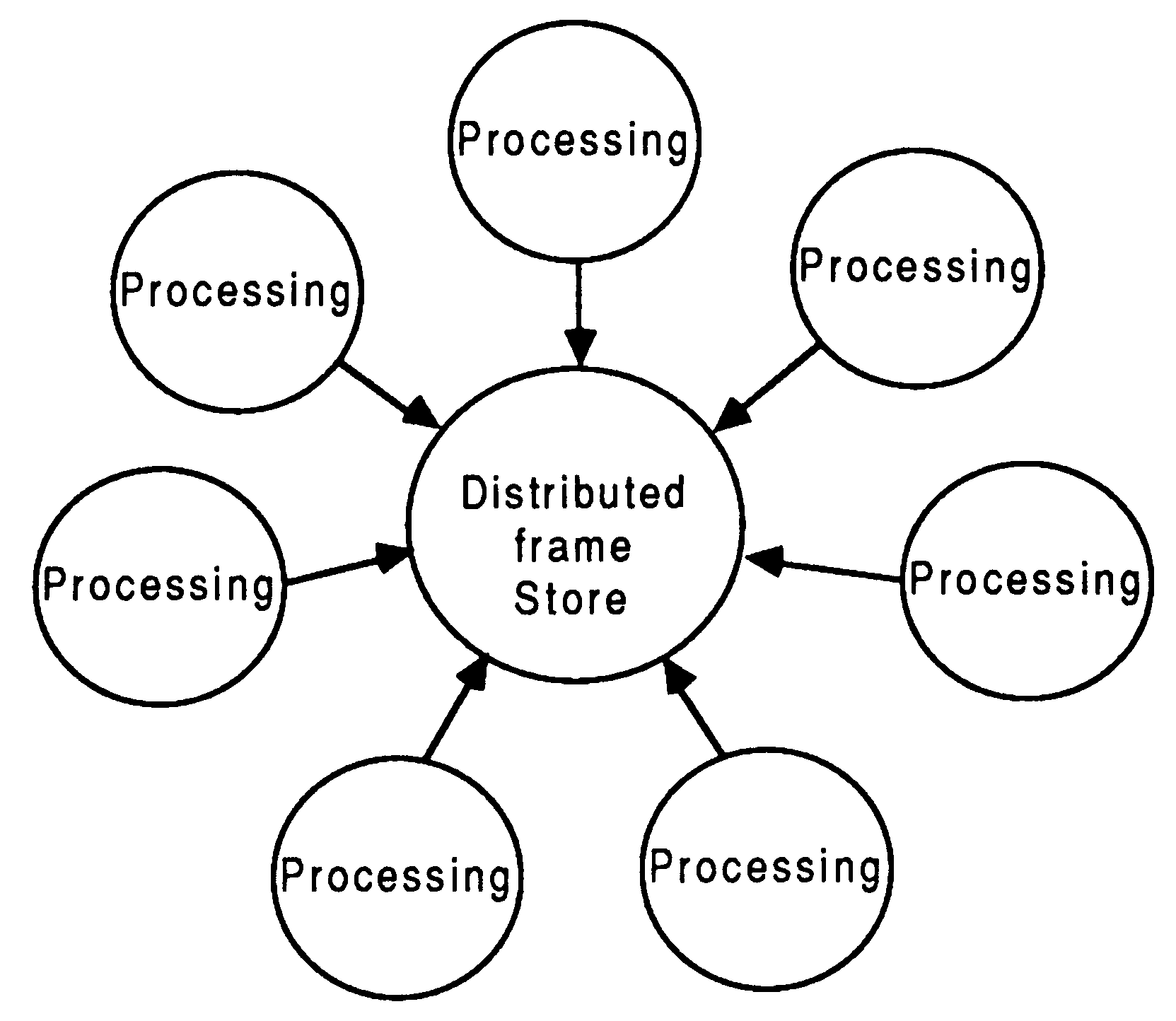
Spatial: The display is broken up into a number of tiles. Each file is distributed to a different processor or a group of processors (see figure 8).
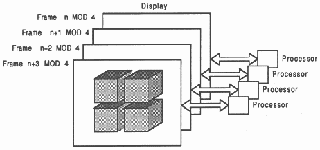
Chronological: This method distributes the entire display to all processors in the system, but only one will display all it’s data at any one time. Each frame of the display is produced by a processor or a group of processors (see figure 9).
Objective: This method distributes different objects in a scene to different processors. This is deceptively difficult - consider the problem of handling hidden and intersecting objects (see figure 10).
Characteristic: This method distributes characteristics of the scene, such as colour, to different processors (see figure 11).
These distribution methods are simplified using the occam model of localised data and process communication, applied with the transputer localised processor bus and interprocessor communication.
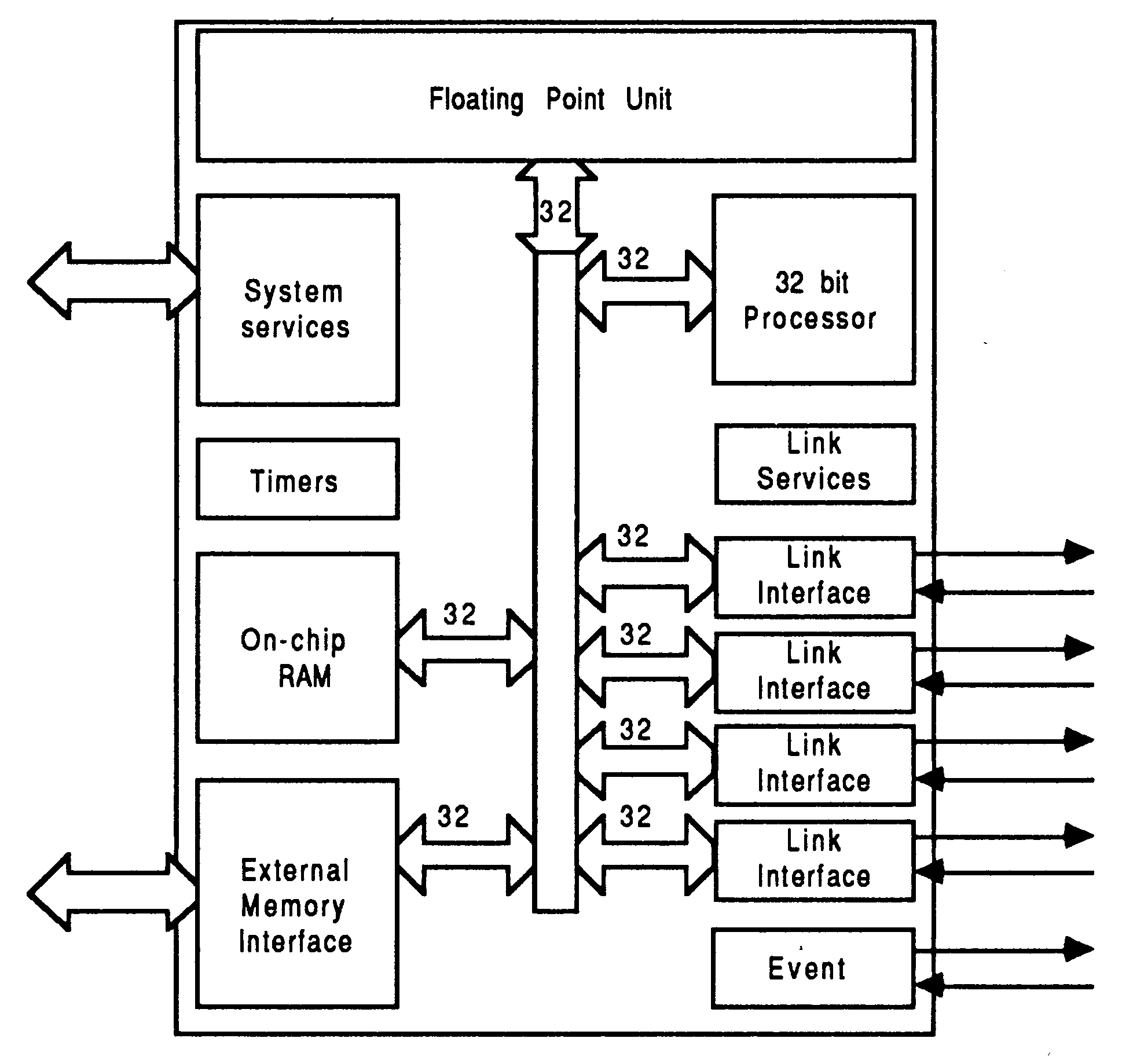
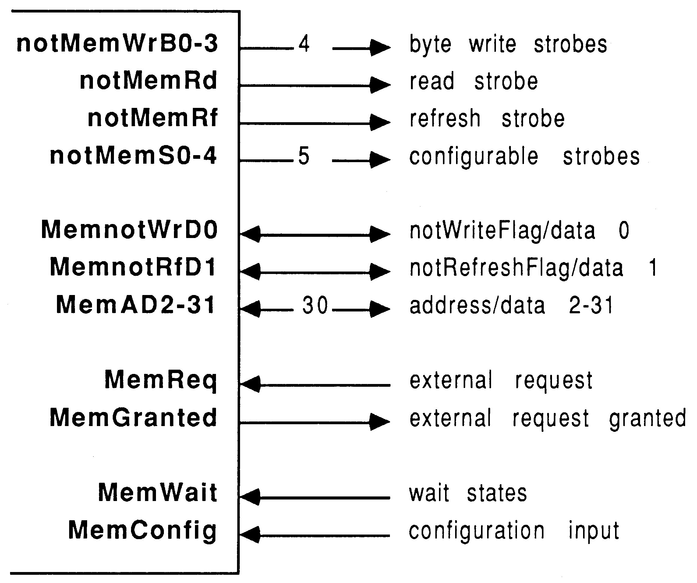
The IMS T800 is the latest member of the INMOS transputer family [1]. It integrates a 32 bit 10 MIP processor (CPU), 4 serial communication links, 4 Kbytes of RAM and a floating point unit (FPU) on a single chip. An external memory interface allows access to a total memory of 4 gigabytes (see figure 12).
The transputer family has been designed for the efficient implementation of high level language compilers. Transputers can be programmed in sequential languages such as C, PASCAL and FORTRAN (compilers for which are available from INMOS). However the occam language allows the programmer to fully exploit the facilities for concurrency and communication provided by the transputer architecture.
The on-chip memory is not a cache, but part of the transputer’s total address space. It can be thought of as replacing the register set found on conventional processors, operating as a very fast access data area, but can also act as program store for small pieces of code.
The 4 serial links on the IMS T800 allow it to communicate with other transputers. Each serial link provides a data rate of 1.7 MBytes per second unidirectional, or 2.35 MBytes per second when operating bidirectional [2].
Since the links are autonomous DMA engines, the processor is free to perform computation concurrently with link communication. With all four links receiving simultaneously, the maximum data rate into an IMS T800 is 6.8 Mbytes per second. This allows a graphics system based around IMS T800s to act as image sinks, accepting pixels down serial links and placing them directly into the frame store.
The IMS T800 FPU is a co-processor integrated on the same chip as the CPU, and can operate concurrently with the CPU. The FPU performs floating point arithmetic on single and double length (32 and 64 bit) quantities to IEEE 754. The concurrent operation allows floating point computation and address calculation to fully overlap, giving a realistically achievable performance of 1.5 Mflops (4 million Whetstones [3]/second) on the 20 MHz part; 2.25 Mflops (6 million Whetstones/second) at 30 MHz.
Among the new instructions in the IMS T800 are those for graphics support. The IMS T800 has a set of microcoded 2-dimensional block move instructions which allows it to perform cut and paste operations on irregularly shaped objects at full memory bandwidth.
The three MOVE2D operations are:
| MOVE2DALL | which copies an entire area of memory |
| MOVE2DZER0 | which copies only zero bytes |
| MOVE2DNONZERO | which copies only non-zero bytes |
The use of these instructions is described more fully elsewhere [2].
The occam language enables a system to be described as a collection of concurrent processes which communicate with one another, and with the outside world, via communication channels. Occam programs are built from three primitive processes:
| variable := expression | assign value of expression to variable |
| channel ? variable | input a value from channel to variable |
| channel ! expression | output the value of expression to channel |
Each occam channel provides a one way communication path between two concurrent processes. Communication is synchronised and unbuffered. The primitive processes can be combined to form constructs which are themselves processes and can be used as components of another construct. Conventional sequential programs can be expressed by combining processes with the sequential constructs SEQ, IF, CASE and WHILE.
Concurrent programs are expressed using the parallel construct PAR, the alternative construct ALT and channel communication. PAR is used to run any number of processes in parallel and these can communicate with one another via communication channels. The alternative construct allows a process to wait for input from any number of input channels. Input is taken from the first of these channels to become ready and the associated process is executed. A full definition of the occam language can be found in the occam reference manual [4].
Transputer Modules [5] or TRAMs are subassemblies of transputers (or other components with INMOS links), a few discrete components, and sometimes some RAM and/or application specific circuitry. All TRAMs:
These TRAM standards make it very simple for users to build customised TRAMs or motherboards with sockets for TRAMs. The TRAM pinout standard is independent of:
If the graphical display processors are implemented as modular transputer compute elements, each with transputer, memory and logic to implement special functions, the problem of designing a distributed graphics system becomes much simpler.
To provide the distributed frame store requirements and any display output type (see section 2.6), different TRAMs are deemed necessary.
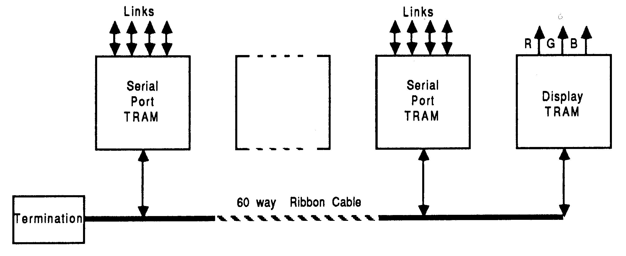
Serial port TRAM: This contains an IMS T800 and all the logic necessary for a complete frame store. It can be connected to other identical TRAMs so that distribution of the frame store becomes a matter of simple replication of this TRAM. This is known as the Serial port TRAM because of the serial nature of the output data.
Display backend driver TRAM: This contains all the logic necessary to drive a particular display type, This TRAM interfaces directly to, and receives it’s high speed data from, the serial port TRAM. This TRAM will be known as the Display Backend TRAM.
Separation of frame store scanning from the processor address and data bus is achieved on the serial port TRAM using video RAMs (see section 9). Video RAMs have a separate serial port (a port in this context means a separate access path to shared data) for video data. This allows the frame buffer to be scanned in a serial fashion without causing significant loss of processor access to the RAM, relieving the arbitration problems associated with conventional RAMs (see section 2.5).
The serial port TRAM supplies a continuous stream of high speed serial data from the frame store. The Display Backend can drive display monitors using this stream of data in a variety of display modes. These TRAMs are connected together by a 60 way ribbon cable, which contains a control bus and a distributed data bus. All serial port TRAMs in the system connect in parallel to this cable (see figure 13).
This section contains a short introduction to the serial port TRAM. A detailed description can be found in section 4.
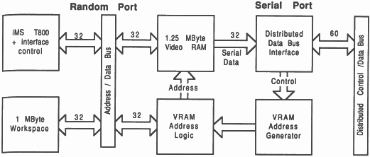
The serial port TRAM (see figure 14) consists of:
A transputer: An IMS T800, which maintains the frame store.
Memory: The standard serial port TRAM contains a total of 2.25 Mbytes of 4 cycle dynamic RAM. Of this 1 Mbyte is standard dynamic RAM and 1.25 Mbytes is Video RAM.
Video RAM address generator: This controls the VRAM serial port addressing. It is in turn controlled by the distributed control bus.
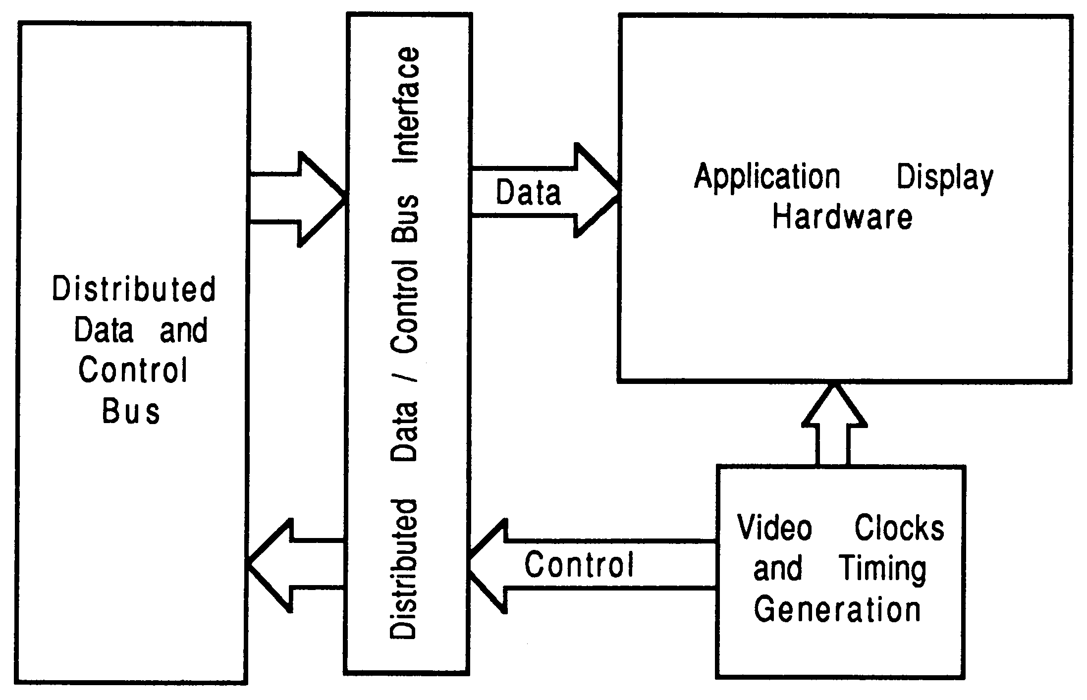
Serial bus interface: This is the distributed serial data and control bus interface. It connects the distributed control bus to the various timing components on the TRAM and the VRAM serial data to the distributed data bus.
Figure 14 shows a block diagram of the serial port TRAM, outlining some of the blocks previously described.
All display TRAMs have a generic architecture. Figure 15 shows the generic block diagram of the display backed TRAM architecture. A detailed description of the Display Backend can be found in section 5.
The Display Backend TRAM consists of:
A transputer link: Communication to this module via at least one INMOS link, as a processor may not be necessary as it is used only for control and initialisation of the backend hardware.
Video system clock generator: This provides the video system clock. The video system is timed from this clock.
A video timing generator: From this, all synchronisation and system control is derived.
Serial control and data bus interface: This drives the distributed serial control bus and takes data from the distributed data bus.
Application specific display hardware: This hardware produces the application specific output derived from the 32 bit input data.
In the short introduction to the serial port TRAM (section 1 and in figure 14) the functional blocks were briefly discussed. This section will discuss the serial port TRAM in more detail.
The serial port TRAM can be considered as a transputer with memory, some of which is dual ported video RAM. The VRAM has a serial and a random access port to the frame store. These two ports can be considered more or less as separate entities, see figure 14. This section will give an overview of the serial port TRAM and then describe each port separately.
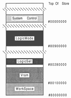
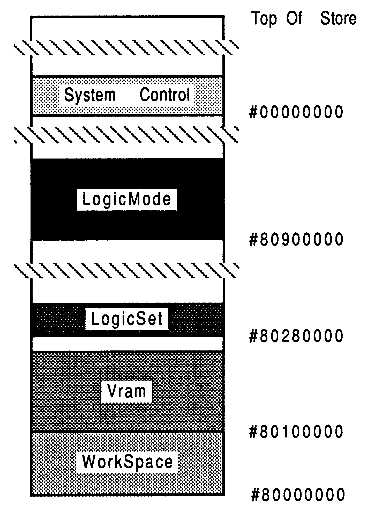
The serial port module has 2.25 Mbytes of usable dynamic RAM. Of this 1 MByte is conventional dynamic RAM and 1.25 Mbytes is dual ported video RAM. Referring to figure 16 the RAM has been placed so that the video RAM abuts the 1 Mbyte of workspace RAM, this allows the video RAM to be used as extra workspace RAM if required.
The video RAM is mapped twice into the decoded memory map so that the special logic modes (marked Logic Mode) used in some video RAMs, which need special interfacing cycling, can be used (see section 9). These special logic modes can be set by writing data to the area of store reserved for this purpose (marked Logic Set). Registers which control the serial port addressing and frame synchronisation are mapped into the positive address space (marked System Control).
The serial port TRAMs frame store is designed around the Packed Pixel architecture (see section 2.3). There are two addressing schemes that can be used with video RAMs, when using packed pixel architecture:
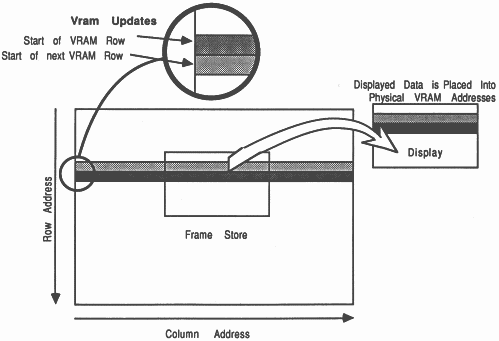
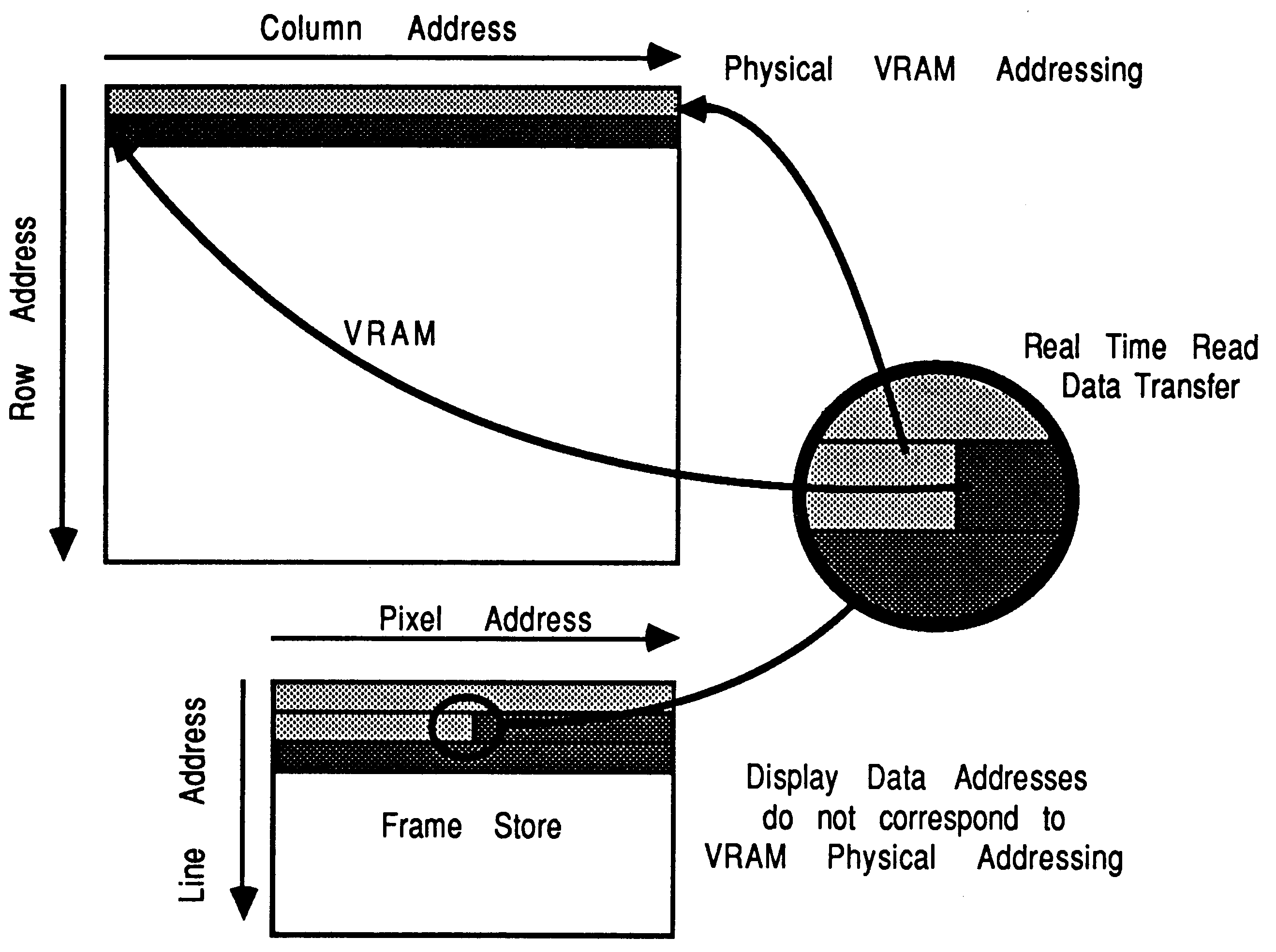
Memory relative: Data is placed into the frame store with addressing related to the physical addressing of the video RAM. Put simply, the VRAM row and column addresses have a direct relationship with the frame stores X and Y coordinates, but the display can have a different horizontal dimension than the frame store. Notice that the maximum width of display is the size of the dual port buffer in the VRAM, i.e. 1024 8 bit pixels (see figure 17).
Display relative: The VRAM row and column addressing have no direct relationship to the frame stores X and Y coordinates. Instead the frame store addressing and the visible display have the same horizontal dimension (see figure 18). This scheme needs the video RAM real time data transfer mechanism (see section 9), which allows the display horizontal dimension to be longer than the VRAM dual port buffer, i.e. longer than 1024 8 bit pixels.
The serial port TRAM normally uses the display relative addressing scheme. When interlace is used, which can be set at initialisation, it is switched into memory relative mode, and the frame store has a fixed horizontal dimension of 1024 bytes (although the display can be smaller). These methods reduce the logic necessary to construct the address generator.
The video RAM can be used for various pixel types and screen sizes. The usage of the frame store entirely depends upon the user software and the backend display TRAM. Recommended mappings are (see figure 19):
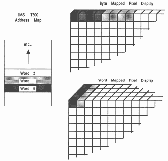
8 bit packed pixels: Pixels mapped as bytes, four pixels per word. This allows 256 colours per pixel with a maximum of 1310720 pixels. This can be used for high resolution CAD, i.e. one serial port module can produce a 1280 by 1024 by 8 bit display, with an appropriate display backend.
32 bit packed pixels: Pixels can be mapped as 32 bit words, allowing a maximum of 232 colours per pixel. One serial port TRAM can have a total of 327680 pixels. Applications include any system that needs real colour displays.
The method of mapping the frame store to the processor can have a profound effect on the performance of the graphical operations a single IMS T800 can achieve. To achieve most efficient use of the IMS T800 performance, pixels should be mapped as either bytes or 32 bit word data types as this takes advantage of the IMS T800s internal datapath representation.
It is useful, when maximising performance in some graphic applications such as animation, to have at least two displays mapped onto the frame store. This allows one to be displayed whilst another is being updated.
To facilitate this, the address of the first pixel at the top left of the display can be preset. This address presetting allows the display to be flipped to alternate areas of the frame store (see section 4.3). Flipping the display during frame flyback allows complete frames to be drawn before being displayed. This prevents disturbing visual artefacts.
The transputer can be informed of the state of the frame flyback condition so as to synchronise the frame flip to the frame flyback period. It is also sometimes necessary to synchronise with other serial port TRAMs in a system when some system wide or global event has occurred. Each serial port TRAM can cause a system event or can respond to it from an external source.
For this reason logic has been included so that the serial port TRAM can be informed when a frame flyback or system event has occurred. This logic uses the IMS T800 Event input (similar to a transputer link but it is only able to convey information about when external events have occurred). Alternatively the transputer can poll some registers which have bits representing the state of these signals.
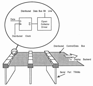
The method of frame store distribution (see section 3.1) can have dramatic effects upon the design of the hardware to implement it. For the serial post TRAM the design rests on the specification of the distributed data bus, which consists of a synchronous (clocked) inverted open-collector bus (see figure 20).
The open-collector arrangement allows any serial port TRAM to output data onto the bus at any time without fear of bus contention. This removes any need for any bus arbitration logic hence, allows arbitrary distribution of screen space amongst an arbitrary number of serial port TRAMs. Each serial port TRAM has enough memory to be able to address any pixel of the display. Since all serial port TRAMs are synchronised any one of them can alter the pixel data presently on the distributed data bus. If any serial port TRAM is not responsible for any particular pixel, it simply writes a null (zero) into that location in the frame store. This fits neatly into the IMS T800 2D block move instructions (see section 3.2), as null has special meaning when moving data with these instructions [2].
This distribution technique is simple, and provides the spatial and characteristic distribution methods described in section 3.1. To further enhance the flexibility of this, an output enable control bit is mapped into the IMS T800 address space. Any serial port TRAM output can be switched off (or nulled) completely. This provides the chronological distribution method discussed in section 3.1.
The objective distribution method also discussed in section 1 has not been implemented due to its complex nature. It is suggested that the reader refer to 6 and 7 both of which deal with distribution of solid object geometry and some implementation methods.
This section will describe the implementation of the transputers access to the frame store. It also describes the mechanisms used to take full advantage of video RAM architecture.
As memory technology progresses, memory speeds increase as well as memory densities. Usually a designer, where possible, will incorporate the logic and PCB tracking necessary for a memory upgrade. To upgrade designs to more memory is quite straightforward, but to upgrade to a higher speed can mean a redesign, an option that can be economically unacceptable.
The IMS T800 allows the designer to upgrade memory speeds by changing the memory interface Configuration (see section 8.9). The serial port TRAM has the configuration data stored in a PAL (programmable array logic) which also controls the IMS T800s speed selection (as this has a bearing on the memory interface timings). This means that a speed upgrade requires only a PAL change (assuming logic delays are taken into consideration).
The upgrade paths allowed for in the design of the serial port TRAM are:
Memory size: An increase in the size of the workspace RAM from 1 Mbyte to 4 Mbytes, using 4 Mbit rams when available. For the 4 Mbit RAMs extra addressing bits were included with no real cost. The upgrade involves a decode PAL and an option resistor (to change an address bit to a decoding PAL). The decoding needs to be changed because the video RAM will be pushed further up the address space.
Memory speed: The speed of the interface can also be changed with the configuration PAL which also contains the speed selection for the IMS T800 as discussed above.
The serial port TRAM has eight different types of memory access:
Internal read/write: This cycle is the fastest. It is internal to the IMS T800 and lasts for a single cycle (50 ns on the 20 MHz transputers)
External read/write: This cycle is the basic external memory cycle. It lasts for four processor cycles (200 ns on the 20 MHz transputer) and consists of a conventional dynamic RAM multiplexed addressed cycle (see figure 21).
Refresh: This is a CAS before RAS refresh cycle (see section 8.5), due to an addressing complication of the video RAMs. The notMemRf strobe is used to cause the relative timings of RAS and CAS to change.
Video update: This cycle is controlled by the video update logic. It allows the video RAM serial port to be updated. The video logic proceeds after gaining control of the data and multiplexed address buses and cycles the video RAM with a serial port update cycle. This cycle only happens infrequently, when data in the serial port is about to run out of data.
Logic operation set: The logic operation unit available in some video RAMs is activated using a CAS before RAS write cycle (see section 9). The logic mode remains set until a Reset Logic Mode or another Logic Operation Set Mode is issued.
Logic operation: The Logic Operation cycle is a conventional RAS-CAS cycle but is six cycles long. This cycle needs a special extended RAS pulse, which is generated from a combination of the interface strobes notMemS1, notMemS2 and notMemS4. This cycle is forced to six cycles using notMemS4 strobe fed back into the Wait input of the IMS T800. This is done as a function of the addressing, and is controlled by a PAL,
Serial port control logic: This cycle allows the transputer to access the serial port control logic. It is initiated when A31 is low. All RAMs are disabled in this cycle.
Configuration: The configuration sequence is a conventional external read cycle that is used only after the transputer has just been reset (see section 8.9). The configuration data is generated from the configuration PAL using the six least significant unlatched address bits. The configuration data is then latched into a single bit of the decode address latch to hold the data until the end of the cycle.
Due to the multiplexed address-data bus of the IMS T800 the addresses are only available at the beginning of the external memory cycle. The addresses have to be demultiplexed from the data (see section 8.3). This is done using the transputer strobe notMemS0 driving the latch enable inputs (marked LE on figure 22) of two ten bit transparent latches. The latches used are high speed CMOS, as these have low propagation delays and have high output drive.
Due to the multiplexed address bus used with dynamic RAMs, the now demultiplexed transputer addresses have to be multiplexed onto the RAM address bus (see figure 22). To achieve this the output enables of the address latches are controlled from a high speed PAL. The outputs from two latches are connected together.
This control is a function of the transputer memory interface strobes notMemS2 and MemGranted (see section 8). MemGranted is used because the video logic needs to drive the multiplexed address bus during a video update and therefore the multiplexer outputs have to be turned off completely.
A slight complication concerning the order of the multiplexed addresses presented to the video RAM, arises due to the way data is stored in the video ram. The most significant address bits are presented as row addresses, which can cause the a problem with the refresh address, which is on the low order address bits (see Memory cycles).
The top address bits AD31, AD23..18 and the Configuration data are latched into a separate eight bit transparent latch. These address bits are used for the decoding.
The RAM is arranged as:
The high speed PAL that controls the operation of the address multiplexer also generates four RAS strobes, one for the workspace RAM and three for the video RAM. Pairs of video RAM banks share RAS strobes The last VRAM bank and the workspace RAM have their own RAS strobe.
The CAS strobes are supplied from another high speed PAL. This essentially is the RAM decoder, having six separate CAS strobes The decoding is a function of the latched addresses A20..18, A31 and the Option input (see Memory upgrades). The CAS strobes are timed from notMemS3 on a External Read/Write cycle.
Decoding with RAS is not essential if a full decode with CAS is used, as in this case, but it has several advantages:
Less heat dissipation: It will cause less heat to generated by the memories. This is so because RAMs consume more current when RAS is cycled, even when not completely selected by a subsequent CAS strobe. Heat dissipation can be a problem in non forced air enclosures.
Speed: Using several RAS strobes instead of one decreases the capacitive loading on the respective strobe, so the strobe can meet critical timings.
This section will describe the implementation of the serial interface on the serial port TRAM.
At the heart of the distributed frame store are two clocks which are synchronous. Both clocks are distributed to all serial port TRAMs in the system. One is known as the sequencer clock and the other is known as the VRAM clock (the VRAM clock can run slower than the pixel rate, so that the 32 bits of data can be multiplexed at a higher clock rate to the display). The VRAM clock is stoppable, controlled by the display TRAM, and is switched off just before the start of, and switched on just before the end of, the horizontal blanking period.
The serial port is built from several distinct groups of logic all synchronised to the previously mentioned clocks:
The address generator: This generates the new serial address for the VRAM during a serial port update. The address generator has tri-state bus drivers connected to the multiplexed address bus of the VRAM.
Address sequencer: This orchestrates control of the address generator during the update the serial port. The address sequencer takes over from the transputers memory interface and then cycles the VRAM in a data transfer cycle.
Pixel counter: This starts the sequencer when serial data in the VRAM is about to run out. It is simply a counter that counts the data read out from the serial port, which resets itself immediately after the update occurs.
Serial bus interface: This is the interface to the distributed data and control bus. This interface is clocked using the sequences clock.
The address generator is used when a video update cycle has been initiated. It provides 19 address bits, some of which are presented to the VRAM during a serial port update cycle (see section 9) and some of which are used as decode selectors. These addresses only form the start address for the serial data, subsequent data is accessed by clocking the VRAM (see figure 24).
The lower 8 bits of the address are fixed but are presetable. This forms the column address to the VRAM during the update cycle. This determines which data appears at the VRAM serial output after the VRAM has been updated.
The next 11 address bits are generated from a preloadable counter that increment just after every update cycle. This address points to the first VRAM row to be accessed after each new frame is started. The lower 8 bits from this form the row address in the VRAM during the update cycle. The top 3 bits of the counter are used to control the serial output enables of the five banks of VRAM, see figure 24. There is no decoding on the update cycle, i.e. all VRAMs are updated at the same time.
The counters top 5 bits are preloaded from a 5 bit register which the user can preset so that the display can start from various addresses of the video ram. This provides the frame flipping mechanism mentioned in section 4.1.
This logic interfaces the address generator to the VRAM and determines the timing of the serial update control strobes. It arbitrates this update cycle between the address generator and the IMS T800s memory interface logic.
The sequencer is designed to update the serial port without interrupting the pixel stream. To do this the pixel counter informs the sequencer that the serial data is about to run out. The entire sequencer operation last for 31 sequencer clocks, (new data appears at the VRAM serial outputs after 30 sequencer clock periods).
The sequencer requests the VRAM address bus by asserting MemReq (see section 8). When MemGranted is asserted by the transputer, the sequences cycles the VRAM in a serial port update cycle. This cycle updates the serial port via the random port when the VRAM strobe DT/OE is brought high synchronised with the VRAM serial clock (see section 9). This is known as Real Time Read Data Transfer, see figure 36.
The serial port of the VRAM wraps around after 256 clocks. It therefore needs reloading every 256 VRAM clock cycles if data is not to be redisplayed. To implement this: The pixel counter signals to the sequencer when the end of serial data is about to occur. This end of data signal knows that the update will occur 30 clock periods later, so it signals the sequencer early.
A slight complication of the sequencer operation concerns the line flyback period. The sequencer must finish its operation before line flyback occurs, otherwise data destined for the start of the next line will be lost. The pixel counter will not cause an update to occur if an end of line is due, so that the update cannot occur during the line flyback period. The timing of this is critical, as the data which finds its way to the display is pipelined twice (at the distributed data bus output driver and at the display TRAM) before getting to the display. This means the pipeline must be precharged with data before the display line starts and emptied before the line ends. To this end, the VRAM clock is turned on two clock periods before the start of the line and switched off two clocks before the end of the line.
The serial port TRAM is designed to function as part of a distributed graphics system. For this reason the control necessary to drive the distributed data bus has to be common to all serial port TRAMs in the system. All clocking and control strobes are distributed using parallel terminated transmission lines.
The transmission lines are driven at the source (Display TRAM) using high speed CMOS logic with high output drive capability. This is terminated with a resistor to ground equal to the characteristic impedance of the transmission cable (this resistance will be anything between 50 and 100 Ohm). All control inputs to the serial port TRAM are short stubs to buffers, which offers little disturbance to the transmission line.
It would be impractical to build a graphics system that is capable of practically any present day graphical display output. It is seasonable that a display TRAM should have application specific display output driving hardware.
This particular display TRAM has been designed with some features that allow it to be used in a variety of applications. This display TRAM has:
A transputer: A IMS T212 is used purely as a logic controller to initialise the video timing logic, colour look up tables and the mode selection.
Distributed control bus interface: This consists of a few transmission line drivers, distributing the control signals to all the serial port TRAMs.
Video clocks and timing generator: The pixel clocks and video timing generation used to synchronise all serial port TRAMs are controlled by the display TRAM.
Three pixel channels: Each display channel converts 32 bits of input data from three distributed data bus inputs into the analogue control signals to drive standard display monitors.
The display TRAM consists of three independent 8 bit pixel channels, all with common clock and video timing generators (see figure 25). Each channel has:
Premultiplexer: An eight bit premultiplexer which links 8 bits of data from channel 0 onto channel 1 and 8 bits of data from channel 0 onto channel 2. This then maps 24 input bits of channel 0 onto the lowest 8 bits of channels 0, 1 and 2.
Input latch: Distributed data bus 32 bit input latch.
Multiplexer: 32 bit input 4 to 1 multiplexer
CLUT: 256 location colour lookup table.
There are three modes that the display TRAM has been designed for:
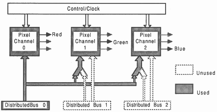
8 bit mode: This mode treats the 32 bit pixel data entering the display TRAM as four 8 bit pixel values. This data is multiplexed to the colour look up table. All three pixel channels operate separately sharing only the distributed control, (see figure 26).
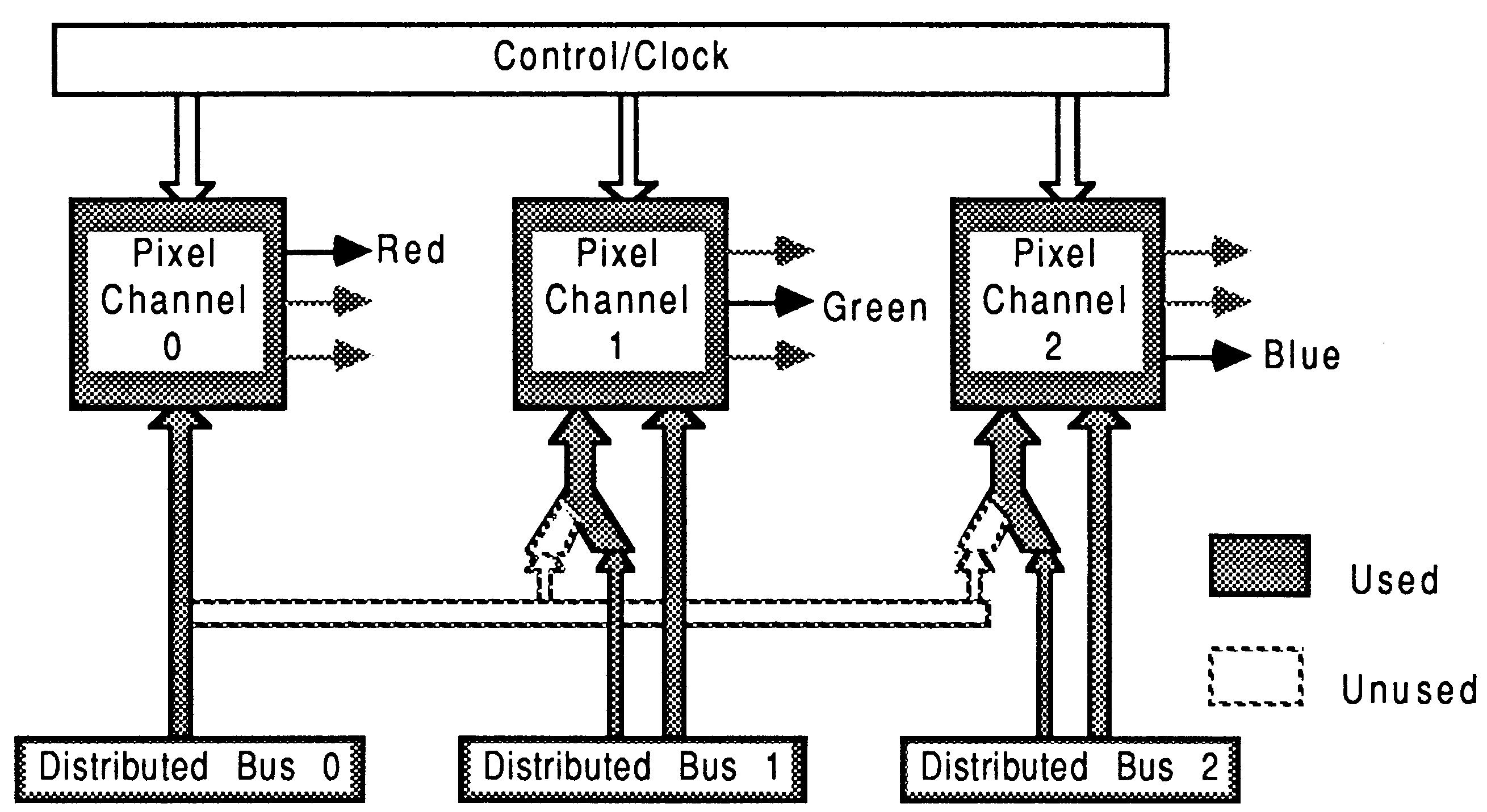
Low resolution 24 bit mode: This mode treats the 32 bit pixel data entering the display TRAM as a single 32 bit word of pixel data. The top 8 bits are not used, leaving the lower 24 bits as pixel data. The three pixel channels contribute to the display, one channel per primary colour (see figure 27).
The 24 bit mode has a different clocking arrangement. Since data is being displayed at the same clock speed (pixel clock) but four times as much data is being used by the display, the input clock speed must be increased, i.e. pixel clock runs at the same speed as the pixel bus. The mode selection can change the clocking arrangements to suit these modes.
High resolution 24 bit mode: This mode is similar to the 8 bit mode, except all three channels are used to provide each of the primary colours (see figure 28).
The serial port TRAM can be used in a varied and non specific manner, but the techniques fall into several distinct classes.
Data generator: The serial port TRAM receives high level graphical commands from another TRAM and satisfies these commands by generating the drawing data into the frame store. The serial port TRAM becomes a programmable graphical drawing engine.
Data sink: No graphical tasks are executed on the serial port TRAM. The serial port TRAM acts purely as a data sink; receiving data from the serial links and places this data directly into the frame store. The frame store data is generated elsewhere on other TRAMs with transputers or specific hardware.
Data generator and sink: A mixture of both the above methods. The performance of the above techniques can be improved by adding more Serial Port TRAMs and distributing the drawing tasks appropriately, thus improving the effective drawing speed or the total serial link bandwidth into the frame store (see figure 29).
Using a combination of serial port TRAMs and the Display TRAM many system configurations can be constructed.
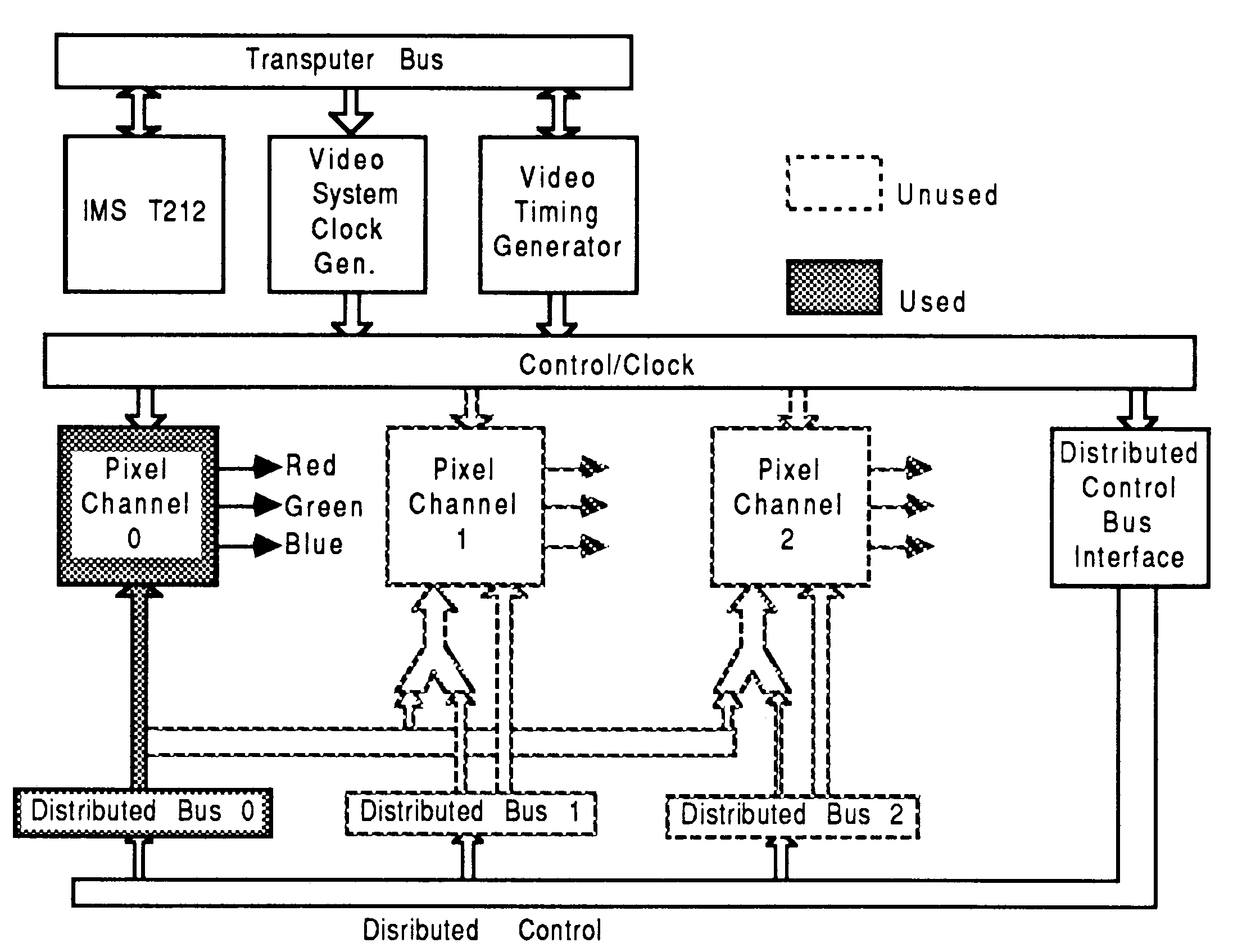
Minimal 8 bit display system: The minimal system consists of a single serial port TRAM and is connected as shown in figure 13. This minimal system provides all that is necessary for a 8 bit pixel (256 colour) graphic display, to a maximum of 1280 by 1024 pixels.
Distributed 8 bit display system: Figure 13 shows a distributed 8 bit graphic display system. This distribution provides increased drawing speed and transputer link bandwidth into the frame store.
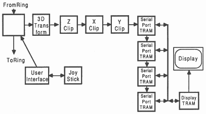
For example in [7], a multi-user flight simulator is described in detail. The system produces an 8 bit 512 by 512 pixel display at 23 frames/sec. The system is based upon a transformation pipeline, and at the end of the pipeline are the polygon shaders. These are transputers that produce display data and send it to the graphics transputer using the data sink method described in section 6.1. An upgrade to higher resolution would consist of placing these polygon shaders onto four serial port TRAMs, turning the display system into a data generator (see figure 30). The display resolution can now be increased with no impact on performance.
Minimal low resolution 24 bit display system: The system in figure 13 can also be used as a low, resolution (maximum of 327680 pixels) 32 bit pixel system. The Display TRAMs premultiplexer is used in this configuration and provides a maximum of 24 bits of output colour (8 bits per primary). Each pixel channel is used as a single primary colour output.
Distributed low resolution 24 bit display system: The system in figure 13 can also provide a low resolution 32 bit display. The display TRAM is set into 24 bit mode as above, but the system provides increased possible drawing and link bandwidth into the frame store as in the distributed 8 bit system, but with more colours.
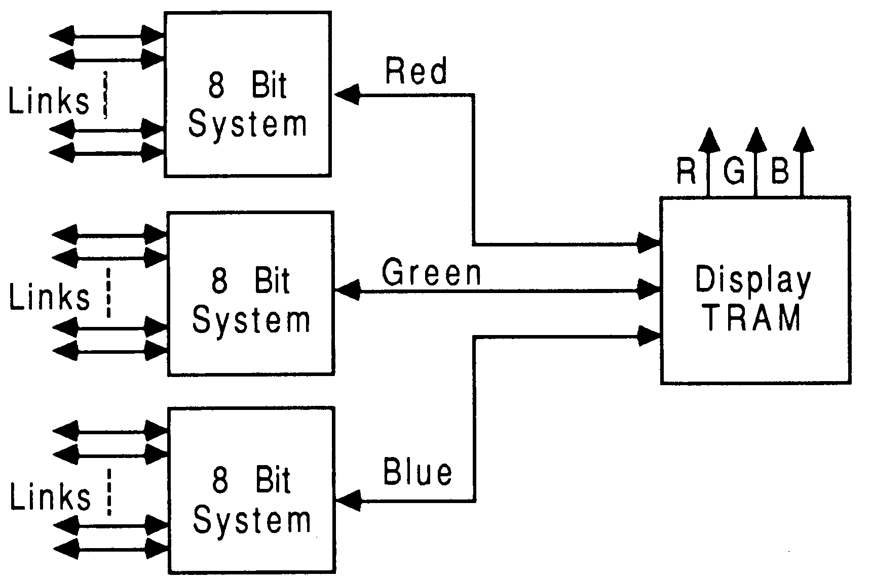
High resolution 24 bit display system: This system (figure 31) is essentially 3 separate 8 bit systems. This method separates the red green and blue components into three 8 bit high resolution display channels as in the 8 bit system. It has all the characteristics of the 8 bit system but each of the 3 pixel channels on the Display TRAM operate independently to provide a primary colour as in the low resolution 24 bit system.
High resolution distributed 24 bit display system: This system (figure 31) is essentially the same as the previous system except that each 8 bit pixel channel is distributed in the same way as the 8 bit system. Again this method separates the red green and blue components into three 8 bit high resolution display channels, but the possible drawing and link bandwidth into the frame store has been increased.
This technical note has shown that the performance of the frame store can be increased without using special hardware by using video RAMs. The video RAM provides a flexible and efficient frame store by mapping the display data directly onto the transputers address map without degradation of bus usage.
This note has looked at the problems associated with frame stores, and has highlighted the problems of single processor bus bottlenecks. It has shown how these bottlenecks can be removed by distributing the frame store, and that this distribution is simplified using transputers.
It has been shown that the large amount of processing necessary to perform typical graphical operations rapidly swamps single processor systems. In high performance systems it becomes necessary to distribute the processing task into smaller more manageable tasks. The complexity and control of this distribution is considerably reduced using transputers and occam, and the distribution of the frame store compliments such a system by providing a convenient interface to the display. Once the distribution has been achieved, adding more transputers into the system, at the display or at the processing front end, can produce any desired system performance.
The IMS T800 has a configurable memory interface designed to allow easy interfacing of a variety of memory types with a minimum of extra components. The interface can directly support DRAMs, SRAMs, ROMs and memory mapped peripherals.
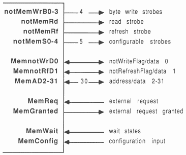
The IMS T800 has a 32 bit multiplexed data and address bus with a linear address space of 4 Gbytes. The interface has:
Figure 32 shows the inputs and outputs for the T800 transputer that are associated with the memory interface.
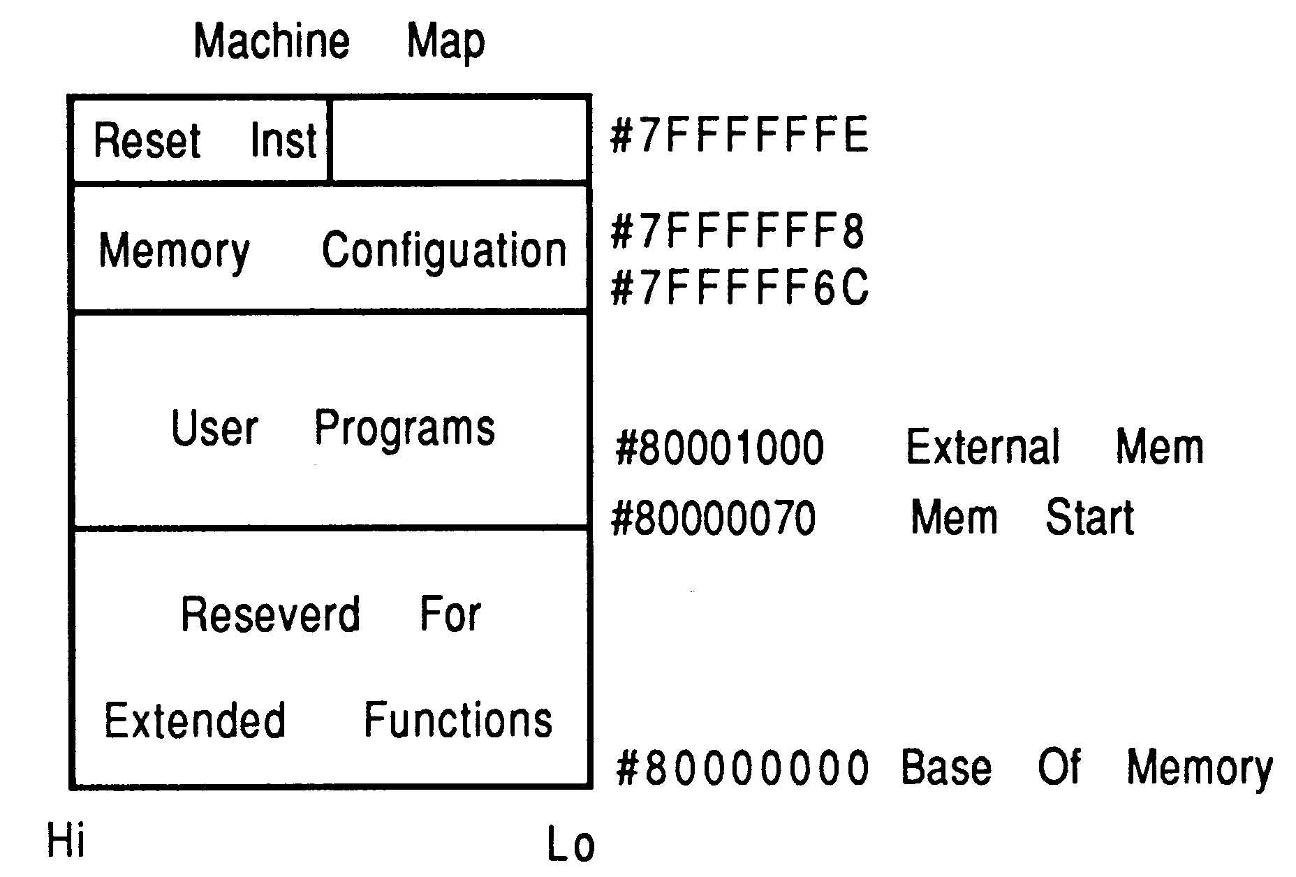
All RAM appears to the IMS T800 as 232 bytes mapped as 32 bit words in a linear signed address space. Addresses, therefore, run from 8000000016 through FFFFFFFF16 to 7FFFFFFF16. As shown in figure 33 the IMS T800 has 4 Kbytes of internal single cycle (50 ns on 20 MHz part) RAM from byte address 8000000016 to 80000FFF16. Of this RAM the first 7016 bytes are reserved for processor use. The IMS T800 has MemStart at 8000007016 and start of external memory at 8000100016.
It is advisable for the address range 8000000016 to FFFFFFFF16 to be used for RAM and 0000000016 to 7FFFFFFF16 to be used for ROM and I/O. If external memory exists it will overlap internal memory, but if the memory map is not completely decoded, it is usually possible to access the hidden external memory at another address.
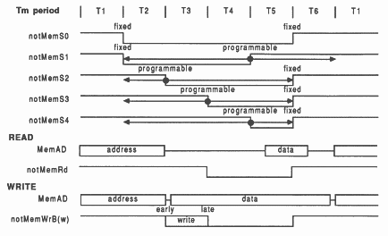
The IMS T800 memory interface cycle has six timing states, referred to as Tstates. The Tstates have the nominal functions:
| Tstate | |
| T1 | address setup time before address valid strobe |
| T2 | address hold time after address valid strobe |
| T3 | read cycle tristate/write cycle data setup |
| T4 | extended for wait states |
| T5 | read or write data |
| T6 | end tristate/data hold |
The duration of each Tstate is configurable to suit the memory devices used and can be from one to four Tm periods. One Tm period is half the processor cycle time, i.e. half the period of ProcClockOut. Thus, Tm is 25 nsec for an IMS T800-20 (20MHz transputer). T4 may be extended by wait states in the form of additional Tms.
With this flexible arrangement, a variety of memory timing controls can be obtained with little external hardware. The bus timing is shown in figure 34.
Every memory interface cycle must consist of a number of complete cycles of ProcClockOut: i.e. it must consist of an even number of Tms. If there are an odd number of Tm periods up to and including T6, an extra Tm shown as ”E” by the memory interface program (see section 8.9) will be inserted after T6.
The use of the strobes notMemS0 to notMemS4 will depend upon the memory system. The rising edge of notMemS1 and the falling edges of notMemS2 to notMemS4 can be configured to occur from 1 to 31 Tm periods after the start of T2. This is summarised in figure 34 and in the table below.
| Signal | Starts | Ends |
| notMemS0 | T2 | T6 |
| notMemS1 | T2 | T2+(Tm*s1) ... or end of T6 if this occurs first |
| notMemS2 | T2+(Tm*s2) | T6 |
| notMemS3 | T2+(Tm*s3) | T6 |
| notMemS4 | T2+(Tm*s4) | T6 |
Where s1, s2, s3 and s4 are the configured number of Tm periods for each respective strobe.
It should be noted that the use of wait states can advance the rising edge of notMemS1 in relation to that of the other strobes. Care must be taken if this signal is being used when Wait states are being used.
The address and data buses are multiplexed onto the MemAd bus. Addresses are available from the beginning of the cycle until the end of T2. Whereupon the MemAd bus will go either tri-state (a passive state) or have data present depending whether a read or write cycle is in progress (if the cycle is a single or multiple byte-write cycle, bytes which are not to be written will go tri-state)
The address bus can be demultiplexed using transparent latches (latches that act as buffers until the latch control is used, whereupon the data becomes held), controlled by notMemS0 directly (not a configurable strobe). The transparent latch will buffer the MemAd bus whilst notMemS0 is not active. When notMemS0 goes active at start of T2, the addresses are held. Using transparent latches makes the demultiplexing simple (using notMemS0 directly) and gives as much address set up time as possible.
During a write cycle, byte addressing is achieved by the four write byte strobes notMemWrB[0..3]. Only the write strobes corresponding to the bytes to be written are active. During a read cycle complete words are read, and the bytes to be used are selected internally. Thus, the two lowest order address bits A0 and A1 are not needed and are not output with the rest of the addresses. However, care must be taken when mapping byte wide peripherals onto the interface, as they are addressed on word boundaries.
The two lowest order data bits during the address period, are used to give early indication of the type of cycle which is in progress:
The notMemWrB strobes can be configured to fall either at the beginning of T3 (early write) or at the beginning of T4 (late write); the rising edge is always at the beginning of T6. Early write gives a longer set up time for the write strobe but data is only valid on the rising edge of the pulse. For late write, data is valid on the falling edge of the strobe but the pulse is shorter.
The IMS T800 has an on-chip refresh controller and 10 bit refresh address counter and can, therefore, refresh DRAMs of up to 4 Mbit capacity (since these are arranged as 1024 rows of 4096 bit columns) without requiring the counter to be extended externally.
Refresh can be configured to be either enabled or disabled. If enabled, the refresh interval can be configured to be 18, 36, 54 or 72 Clockln periods; though if a refresh cycle is due, the current memory cycle is always completed first. The time between refresh cycles is thus almost independent of transputer speed and the length of memory cycles.
Refresh cycles are flagged by notMemRf going low before T1 and remaining low until the end of T6. Refresh is also indicated by MemnotRfD1 going low during T1 and T2 with the same timing as address signals. The address output during refresh is:
| AD0 | = MemnotWrD0 | high, indicates a read |
| AD1 | = MemnotRfD1 | low, to indicate refresh |
| AD2 - AD11 | refresh address | |
| AD12 - AD30 | high | |
| AD31 | low |
During refresh cycles, the strobes notMemS0 - notMemS4 are generated as normal.
Several choices for the designer exist for refresh schemes with the IMS T800. These are
Where:
CAS: Refers to the Column Address Strobe input on the dynamic RAMs.
RAS: Refers to the Row Address Strobe input on the dynamic RAMs.
As all RAMs need to be refreshed simultaneously, all RAMs are RAS selected. As RAMs will consume current when RAS goes active, this is usually the most power hungry cycle of a dynamic RAM interface.
Care has to be taken to ensure that the power supply is not left with a problem of supplying high current surges at refresh, and thereby causing a power supply noise. This can be a particular problem if many transputers with lots of dynamic RAM are used with a common power supply. The refresh may well be nearly synchronous due to the common reset signal. This problem will be made worse if the transputers have a common input clock. The clocking may be near synchronous (albeit on different phases due to the phase locked clock multiplier on each transputer).
It is suggested that large capacitors are used as near to the dynamic RAM as possible, as this will reduce the supply noise to acceptable levels.
Memory cycles can be extended by wait states. MemWait is sampled close to the falling edge of ProcClock Out prior to, but not at, the end of T4. If it is high, T4 is extended by additional Tms (shown as ’W’ by the memory interface program). Wait states are inserted for as long as MemWait is held high, T5 proceeds when MemWait is low. Note that the internal logic of the memory interface ensures that, if wait states are inserted, T5 always begins on a rising edge of ProcClockOut: so the number of wait states inserted will be either always odd or always even, depending on the memory configuration being used.
Direct memory access (DMA) with the IMS T800 has been implemented in the following way.
MemReq can be asserted asynchronously (at any time) with respect to ProcClockOut, but to guarantee DMA, MemReq must be set up two periods Tm before end of T6. MemReq will be sampled at at the final Tm period of T6 of a refresh or external memory cycle when ProcClockOut is low. If the IMS T800 is accessing internal RAM or is idle, MemReq is sampled during the low period of every ProcClockOut and internal memory accesses will not be affected by this DMA activity.
When MemReq has been sampled high, two Tm periods after ProcClockOuts next rising edge, the address bus is tristated and all strobes go inactive. One Tm period later MemGranted is set high to indicate a DMA cycle is in progress. After this MemReq is sampled at each low period of ProcClockOut and if found to be low MemGranted will be removed synchronously at the next falling edge of ProcClockOut.
A few points to note about DMA:
This is always worth a mention, as it is frequently overlooked. All buffered memory strobes and multiplexed addresses should be series terminated with 25 to 50 Ohm. This prevents negative voltage spikes on address and control pins. It cannot be overstressed that negative spikes can cause random memory failures, especially on the higher density RAMs.
The unbuffered data bus need not be terminated as the transputers output drive pads have been designed to prevent the fast edges associated with negative excursions.
A memory interface configuration is specified by a 36 bit word and is fixed at reset time. The IMS T800 has a selection of 13 pre-programmed configurations. If none of these is suitable, a different configuration can be selected by supplying the complement of the configuration word to the IMS T800s MemConfig input immediately following reset.
A pre-programmed configuration is selected by connecting MemConfig to MemnotWrD0, MemnotRfD1, MemAD2-MemAD11 or MemAD31. Immediately after reset, the IMS T800 takes all of the data lines high and then, beginning with MemnotWrD0, they are taken low, at intervals of two Clockin periods, in sequence. This is the internal configuration scan.
If MemConfig is high at the start of this scan, an internal configuration is to be selected. The selection is accomplished by MemConfig going low when the IMS T800 pulls a particular data line low, the configuration associated with that data line is then used.
If, at the beginning of the scan, MemConfig is sensed low before MemnotWrD0 goes low, an external configuration is selected. To aid this when an external configuration is used the configuration data is expected to be inverted so that a single inverter between a MemAd pin and the MemConfig signals an external configuration from ROM.
After the scan, the IMS T800 performs 36 configuration read cycles from locations 7FFFFF6C16 to 7FFFFFF816. If an internal configuration was selected these reads are ignored. If an external configuration has been selected, each of the configuration read cycles will latch one bit of the configuration data into the MemConfig input from an external source.
Using an internal configuration has the advantage of requiring no external components, only a connection from MemConfig to the appropriate data line.
However, selecting an external configuration can also be very economical in component use if the configuration data is stored in a PAL and this PAL is used for other purposes concerning the low order address bits.
If the transputer is booting from ROM, the ROM must occupy the top of the address space. One bit of the memory configuration data can be stored in each of the 36 addresses mentioned above and the only additional hardware required is an inverter connecting the appropriate data line (usually MemnotWrD0) to MemConfig. MemConfig is thus held low until MemnotWrD0 goes low and is fed with the inverse of the configuration data during the 36 read cycles. Alternatively, the inverted configuration data can be generated from A2-A7 by a PAL.
The INMOS Transputer Development System includes an interactive program which assists in the task of memory interface design. The program produces timing diagrams and timing information so that the designer can see the effects of varying the length of each Tstate and the positions of the programmable strobe edges. Of course, the program cannot allow for external logic delays and loading effects as these are system dependent but it does assist greatly in preliminary design. (It has sometimes been considered an essential tool in designing the interface configuration data).
A foolproof method to produce the PAL equations for the configuration data is to modify the configuration data page generated by the memory interface configuration program.
Recent developments in RAM design architecture have made available a cost effective dual ported Video RAM. The video RAM has a secondary set of output selector register sets (see figure 35) controlled by an external serial clock.
This extra selector is able to operate totally asynchronously to the normal selector register set. These two register sets are referred to as the access ports to the RAM bulk, the random access port and the serial access port. The serial access port accesses data in a sequential manner, which needs to be updated when data runs out using the special update cycle from the random port.
The random access port is similar to conventional dynamic RAMs except for the extra function of sequencing the OE (Output Enable) pin. This extra function is called a Data Transfer, hence the pin is renamed DT/OE.
Sequencing the DT/OE pin on a random access causes data transfer from the RAM to the serial port. Once the serial port is updated it can proceed to output data without recourse to the random port, until it needs new data (see figure 36).
The update cycle is the only time that the serial port and the random port interfere with each others operation, but because so much data is read into the internal register sets, this interference happens only occasionally, i.e. every 256 serial port access cycles. This means that a frame store directly mapped into a processors address map will use very little of the processors access to memory to refresh the display.
Some video RAMs have an internal logic operation unit (see figure 37). This unit can be set into particular modes by using a special CAS before RAS write cycle. The modes are selected by writing data to various locations using this special cycle. The data written is used as a write mask when writing subsequently to the RAM.
This mechanism allows a whole series of logic operations, such as Xor, Or, etc, to be carried out transparently during a write cycle. The RAM takes advantage of the fact that write accesses to dynamic RAMs are essentially read-modify-write cycles internal to the RAM. These modes are programmable and include a write-per-bit data mask.
[1] IMS T800 Architecture, Technical Note 6, INMOS Limited
[2] Notes on Graphics Support and Performance Improvements on the IMS T800, Technical Note 26, INMOS Limited
[3] Lies, Damned Lies and Benchmarks, Technical Note 27, INMOS Limited
[4] Occam 2 Reference Manual, INMOS Limited, Prentice Hall, ISBN 0-13-629312-3
[5] Dual Inline Transputer Modules (TRAMs), Technical Note 29, INMOS Limited
[6] High Performance Graphics with the IMS T800], Technical Note 37, INMOS Limited
[7] A Transputer Based Multi-User Flight Simulator, Technical Note 36, INMOS Limited