|
|
| Module motherboard architecture _____________________________________________________________________ |
| Trevor Watson February 1988 |
Inmos transputer modules are designed to form the building blocks of parallel processing systems. They consist of printed circuit boards in a range of sizes which typically hold a member of the transputer family of processors, some memory and perhaps some application specific circuitry. A module needs only a 5 volt power supply and a 5MHz clock to operate. These are supplied to the module through pins on the periphery of the board. Other pins bring out the transputer’s serial links and reset, analyse and error signals. Some modules can control a subsystem of other modules through another set of pins. The Dual-In-Line Transputer Modules (TRAMs) document [1] provides a complete specification of Inmos transputer modules.
In order to use modules as parallel processing building blocks Inmos has developed a range of motherboards. While these boards provide access to transputers from a number of different host machines, they have a common architecture to allow control and interconnection of potentially large numbers of transputers. This document describes the generic architecture of module motherboards. It is recommended that this specification is followed when designing in order to preserve compatibility with INMOS module motherboards.
The INMOS range of module motherboards has a common architecture making it easy to build and configure systems consisting of large numbers of transputer modules. The goals aimed at in the design of the module motherboards, and the architecture developed to achieve them, are described below.
The main goals aimed at in the design of module motherboards are:
In order to achieve the design goals outlined above, a standard architecture is adopted for all module motherboards. The rest of this document describes the motherboard architecture in detail, but the salient features are given below.
Transputers communicate with each other via serial links operating at 10 or 20Mbits/s. The module motherboard architecture facilitates the interconnection of links between transputer modules by providing a standard hardware link configuration and allowing software configuration using IMS C004 programmable link switches. Links should be interconnected by properly terminated transmission lines (PCB trace or cable) having a characteristic impedance of 100 Ohm. Connecting INMOS links [2], gives full details on all aspects of connecting links.
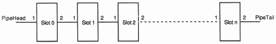
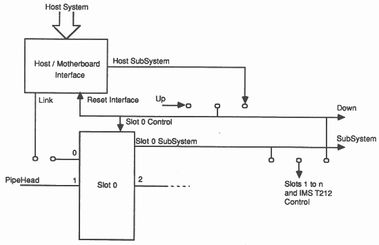
Each module resides in a module slot which provides two sockets that take the 16 pins of a size 1 module. A motherboard may have any number of module slots, determined only by the physical size of the board. The slots are numbered starting at slot 0.
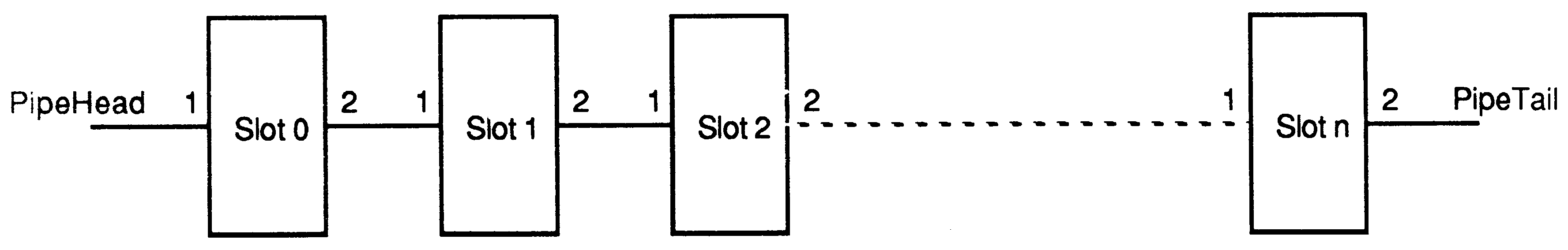
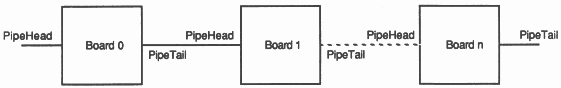
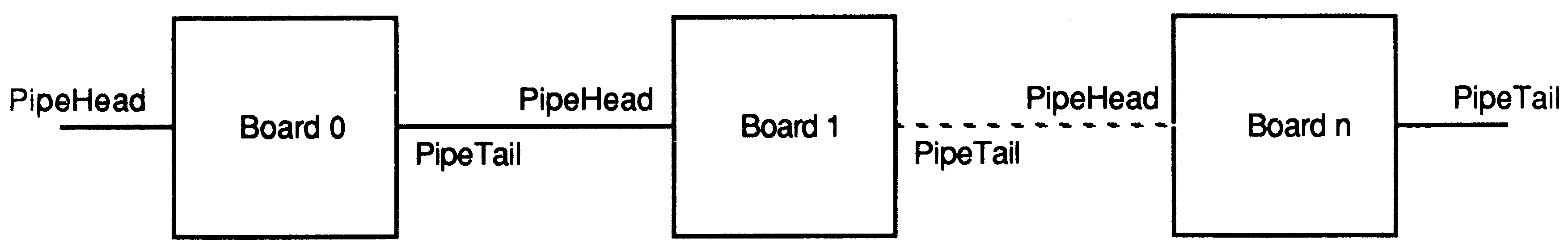
All the modules on a motherboard are connected in a pipeline as shown in Figure 1. Link 2 of the module in slot 0 is connected to link 1 of slot 1 and so on for the rest of the pipeline. Link 1 of module slot 0 (Pipehead) and link 2 of the last module slot (Pipetail) are brought out to an edge connector thus enabling the pipelines of any number of boards to be chained together by connecting Pipehead of one board to Pipetail of the next. See Figure 2.
Some applications may not require a full complement of modules or may use size 2 or larger modules which take up more than one slot, but use only one slot for electrical connection. In either case the pipeline will be broken unless steps are taken to keep it intact. A pipe jumper is a small connector used for this purpose. See Figure 3. It plugs into an unused module slot and connects link 1 of that slot to link 2 of the same slot, thus preserving the pipeline.
An IMS C004 programmable link switch is used for software configuration of links. This device is a crossbar switch which can handle up to 32 links. It can connect any of the 32 link inputs to any of the 32 link outputs under software control from a separate configuration link.
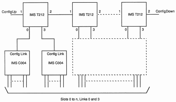
Links 0 and 3 of each module are taken to an IMS C004 or a number of IMS C004s, depending on the number of links. Links may be taken from an IMS C004 to an edge connector to allow links from one motherboard to be connected to those of another.
The number of IMS C004s required on a particular motherboard depends on the number of modules the board can hold. The exact arrangement of IMS C004 links is not specified here in order to give the designer maximum flexibility for his particular application. The only restriction Is that links 0 and 3 of each module are taken to a C004. This may be done in a number of ways. For example:
Each IMS C004 on a motherboard is controlled from an IMS T212 16-bit transputer as shown in Figure 4. An IMS T212 can control up to two IMS C004s via its links 0 and 3. Links 1 and 2 of each IMS T212 are used to connect the transputers in a configuration pipeline. Link 1 of the first IMS T212 on the board is taken to an edge connector designated ConfigUp; link 2 of the last IMS T212 in the board’s configuration pipeline is also taken to an edge connector designated ConfigDown. In this way the configuration pipelines of any number of motherboards may be chained together by connecting ConfigDown of one board to ConfigUp of the next, enabling a network of transputer modules spread over several boards to be configured from software.
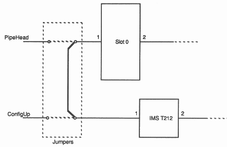
The IMS C004 configuration data may come from software running on a module residing on the first motherboard in the system. It is therefore necessary to be able to connect a link of that module to the board’s configuration pipeline. A jumper provides the option of connecting link 1 of the first IMS T212 in the configuration pipeline either to ConfigUp or to link 1 of module slot 0. in the latter, the jumper also disconnects PipeHead on the edge connector from slot 0 link 1. This is shown diagrammatically in Figure 5.
The hardware configuration described in Sections 3.2 and 3.3 provides the standard architecture recognised by the Module Motherboard Software (MMS), a software package available from INMOS which allows easy configuration of the IMS C004 link connections.
The MMS takes a list of link connections that are hardwired on the board together with a list of the required ’softwired’ connections and generates the configuration details for each IMS C004. For each board in the system, the user can:
The MMS is described in detail in the MMS2 User Guide [3].
The subsystem control function of the module motherboard architecture allows hierarchical control of networks of transputers. It enables a module capable of driving a subsystem to reset or analyse a network of modules and to handle errors in the network. The driving module can itself form part of a network which is controlled by another module. In this way a hierarchy of control is made possible.
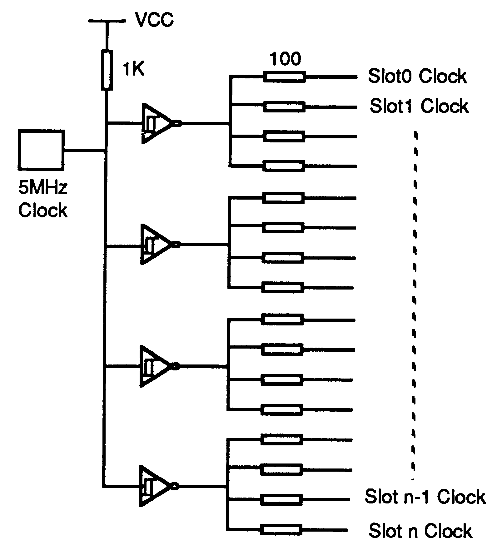
Each module on a motherboard requires a 5MHz clock. The module motherboard specification provides a scheme for distributing the clock signal from a single crystal oscillator to all the modules on a motherboard.
Three signals are provided by transputers for the purpose of allowing system control: Reset, Analyse and Error. The Reset and Analyse inputs enable the transputer to be initialised or halted in a way which preserves its state for subsequent analysis. The transputer Error signal is connected directly to the processor’s Error flag. See the Transputer Reference Manual [4] for a detailed description of these signals.
A transputer module has a similar set of signals: module Reset and Analyse are connected directly to the respective pins on the transputer; the transputer Error pin is taken to a transistor on the module to produce an open collector notError signal that can be wire-ORed with the notError signals of other modules.
Some modules are capable of controlling a subsystem of other modules. They have three extra pins: SubSystemReset, SubSystemAnalyse and notSubSystemError, which are controlled by the on-module transputer through latches in memory. These pins are connected to the Reset, Analyse and notError pins of the modules in the subsystem being controlled. The subsystem can then be reset or analysed by asserting the relevant signal of the subsystem controller module. The subsystem’s ORed notError signal can also be monitored by the controlling module.
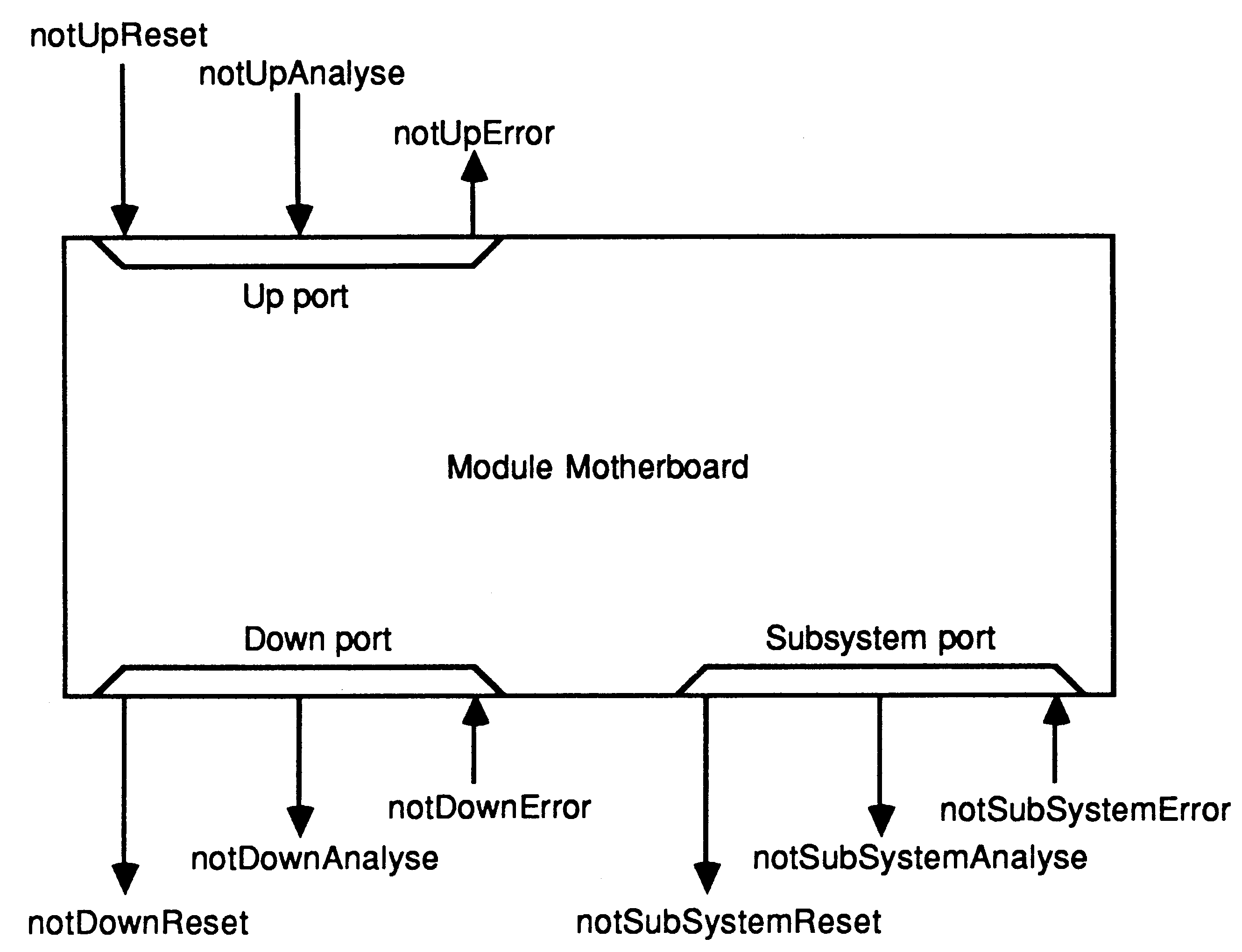
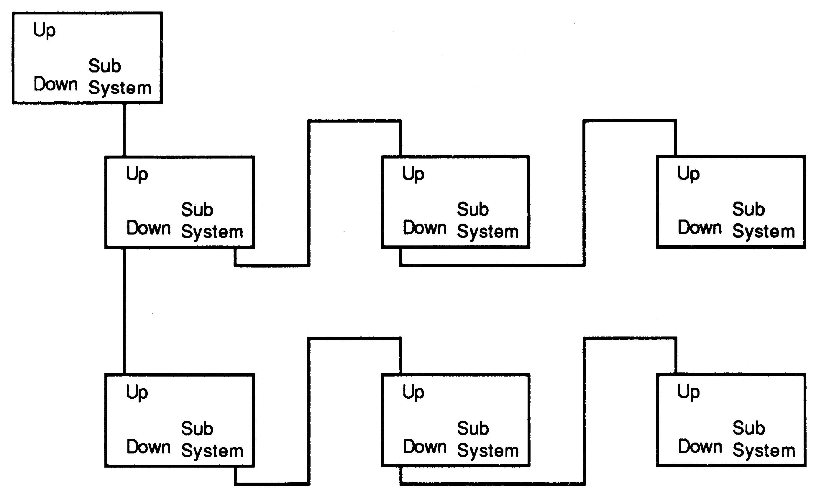
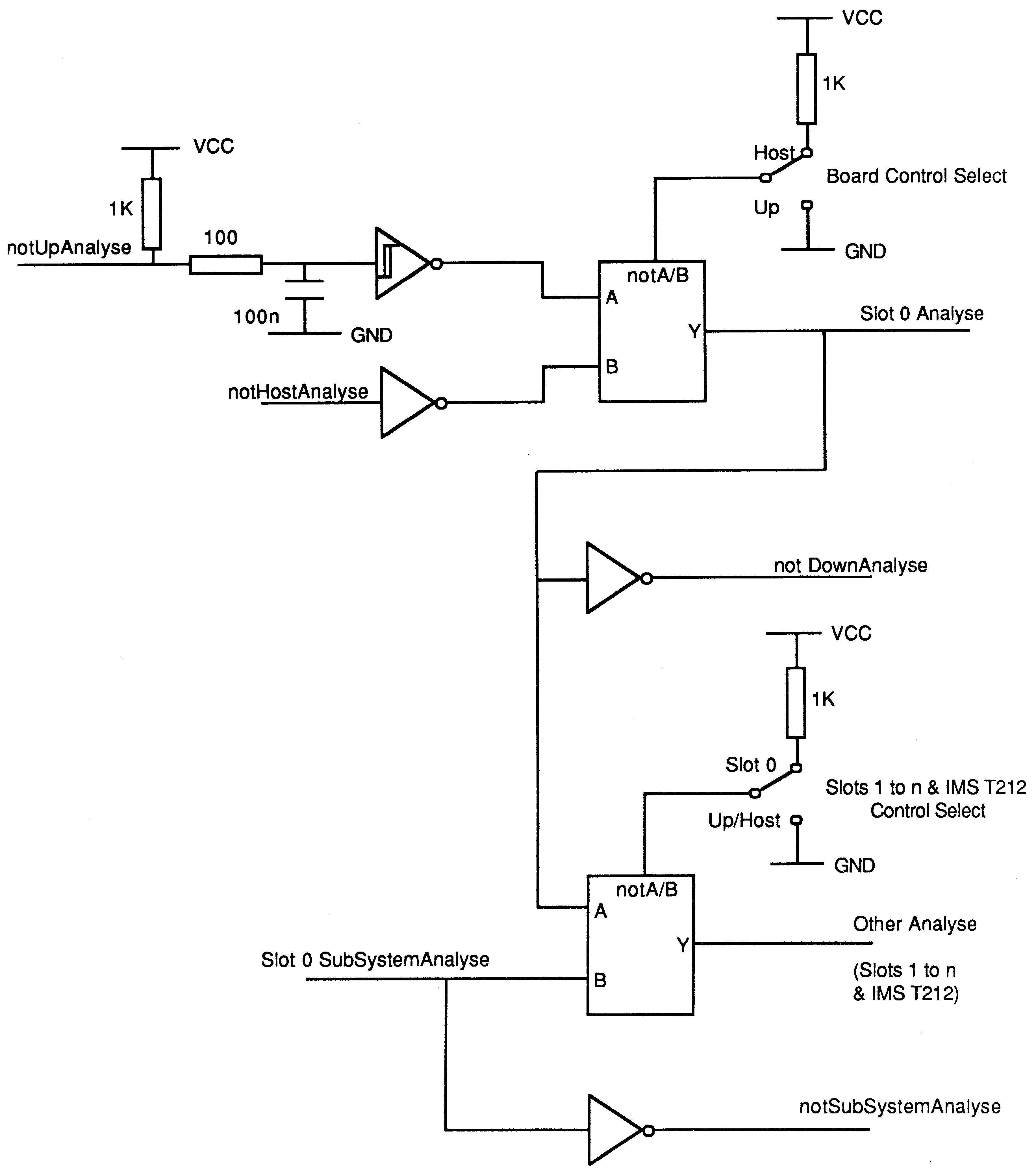
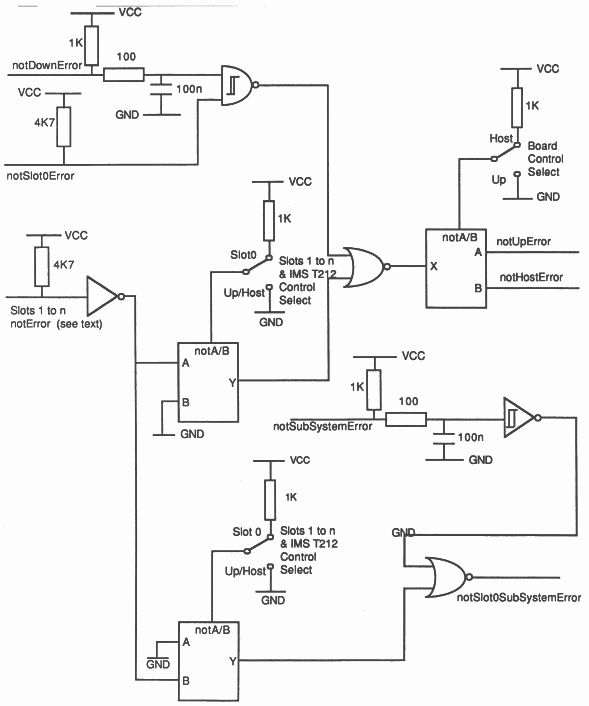
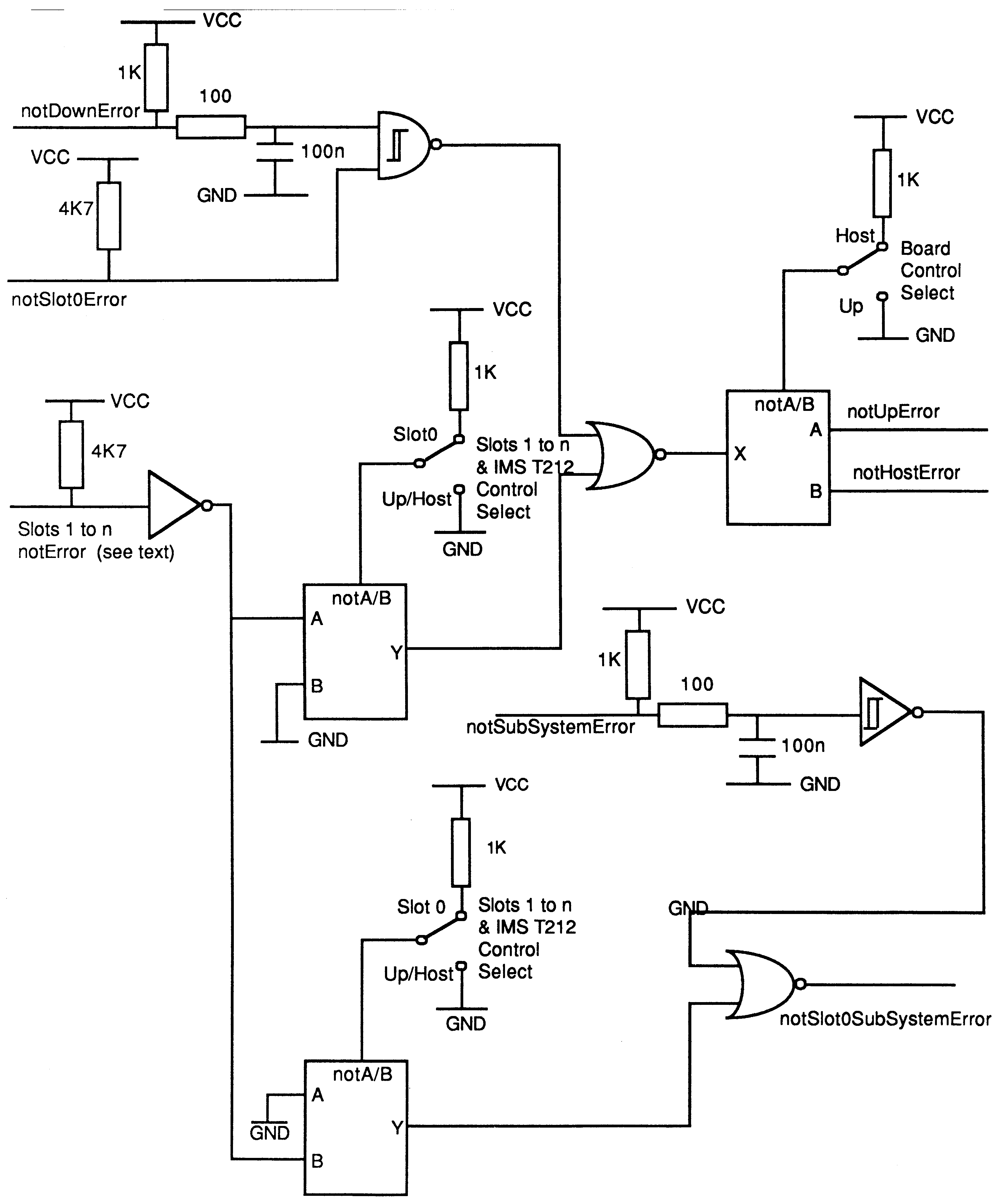
A module motherboard has three ports that provide hierarchical control: Up, Down and Subsystem (see Figure 6). Each port appears at an edge connector and has three active-low signals: notReset, notAnalyse and notError. A board is able to control a subsystem of other boards by connecting its SubSystem port to the Up port of the next board. Boards in a subsystem are chained together by connecting the Down port of one board to the Up port of the next board. A board within a subsystem is in turn able to control another network through its SubSystem port.
Figure 7 shows how a board can be connected to a subsystem of boards.
The notReset and notAnalyse signals flow from SubSystem of one board to Up of the next board. From there, they go directly to Down. They are also logical ORed with that board’s SubSystem Reset and Analyse latches and then pass to the SubSystem port. The notError signal passes from a board through its Up port. If it is connected to the Down port of the board above, it is logical ORed with that board’s Error signal and passed to the Up port. If it goes to the SubSystem port of the board above, the Error signal is not passed on, but is handled by that board. (Figures 10, 11 and 12 show the module motherboard system control logic.)
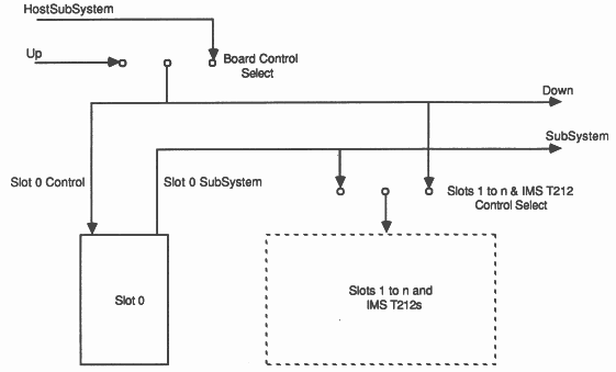
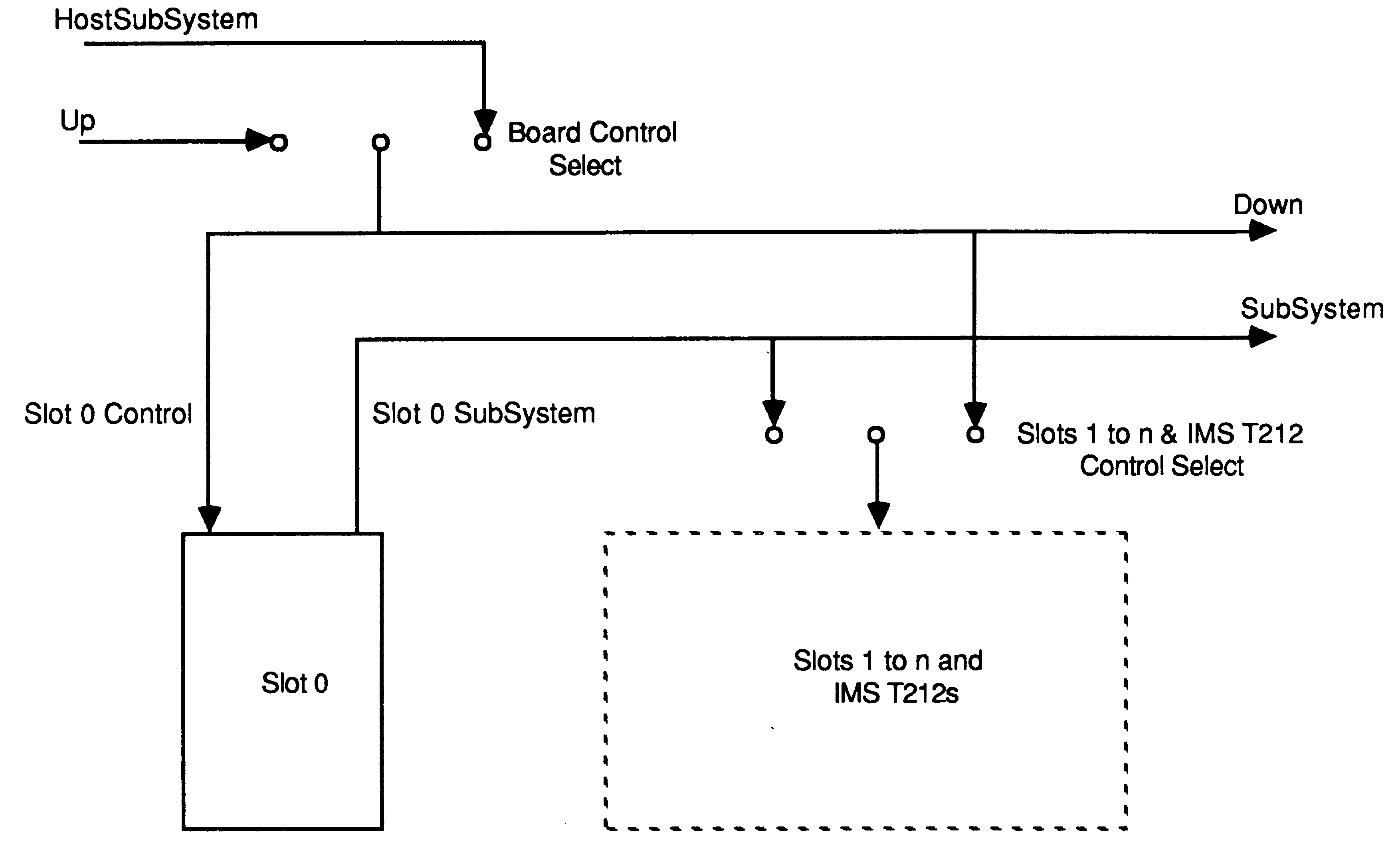
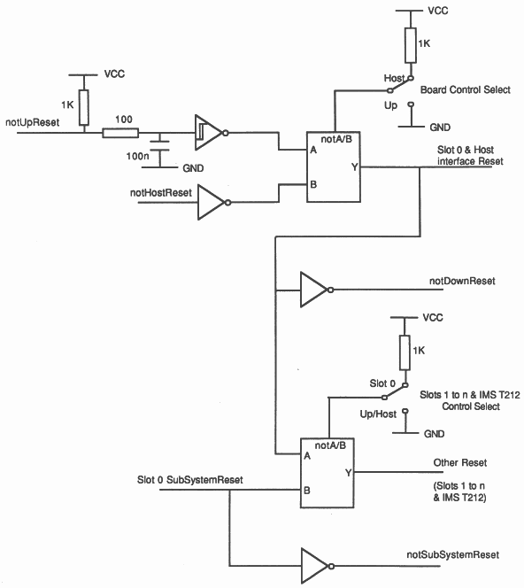
If there are n slots on a motherboard, modules in slots 1 to n may be controlled from either the Up port (or a host machine if the motherboard has an interface to one, see Section 5) or may be part of a subsystem controlled by a suitable module in slot 0. The source of control is determined by a jumper or switch, as shown in Figure 8.
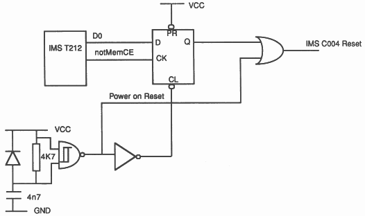
The on-board IMS T212(s) may be reset and analysed from the same source that controls slots 1 to n. The Error pin of the IMS T212(s) is not connected.
A power-on reset circuit is required for the IMS C004(s) on board. An IMS C004 may then be reset at power-on or by the IMS T212 controlling it. Each IMS T212 has a latch mapped into its memory space. See Figure 9. This enables software running on the IMS T212 to reset the IMS C004 either by setting the latch or by sending a reset message to the IMS C004 Configuration link.
Figures 10, 11 and 12 show the logic required for Reset, IMS C004 Reset, Analyse and Error, respectively. These diagrams provide a logical description only: the actual implementation is left to the individual designer. It is important, however, to include the passive components indicated in the diagrams. The 1K pull-up resistors on the notUpReset, notUpAnalyse notDownError and notSubSystemError signals are necessary to ensure that if these signals are unconnected they are not left floating, but are deasserted. The 4K7 pull-up resistors are required to wire-OR the open collector notError signals from the module slots. Note that the Dual-In-Line Transputer Modules (TRAMs) document specifies a maximum of ten notError signals should be wire-ORed together. The combination of each 100Ohm resistor and 100nF capacitor filters out noise on the notUpReset, notUpAnalyse, notDownError and notSubSystemError signals coming from off the board.
To improve noise rejection, it is recommended that Schmitt gates are used to receive signals from other boards. These gates should use bipolar technology (e.g low power Schottky 74LS series TTL). It is also recommended that gates driving signals off the board are capable of providing a full output voltage swing from 0V to 5V, e.g. HCT series gates.
The Reset logic (Figure 10) uses the Board Control Select switch and multiplexer to select whether Slot 0 and the Down port are reset from the Up port or from the host. The Slots 1 to n & IMS T212 Control Select switch and multiplexer determine whether Slots 1 to n and the IMS T212s are reset from the Slot 0 SubSystem port or from the Up port or the host. A similar arrangement is used for the Analyse logic (Figure 11).
In the Error logic (Figure 12), the Slots 1 to n & IMS T212 Control Select switches and multiplexers select whether notError from Slots 1 to n is passed either to the Slot 0 SubSystem port or to the Up port or the host. The Board Control Select switch and decoder determine whether Slots I to n notError, notDownError or notSlot0Error are passed to the Up port or to the host.
Board Control Select and Slots 1 to n & IMS T212 Control Select correspond to the conceptual switches in Figure 8.
A 5MHz, TTL compatible clock signal is required for each module slot, IMS T212 and IMS C004 on board. Since the clock must be distributed to a number of modules and devices the buffering scheme shown in Figure 13 is used to minimise distortion of the clock waveform caused by excessive loading and transmission line effects. This is a star configuration and it may be extended indefinitely by adding more buffers at the star points which may drive further buffers, and so on until the required number of clock signals are derived. The length of any pcb trace carrying a clock signal should be limited to 30cm.
Some module motherboards may require an interface to a host machine or system that is not transputer based, e.g. the IBM PC, VMEbus or Futurebus. Because the implementation of the interface is specific to the host system, it is not defined here. However, it should allow the system to access the module pipeline and control a subsystem of modules.
The host system accesses the module pipeline via Slot 0 Link 0, as shown in Figure 14. It is beyond the scope of this document to define the implementation of the host to link interface, but it might consist of an INMOS link adapter, the registers of which may be mapped into the host’s address space, or it may involve the use of dual-ported RAM shared between the host and a transputer.
The interface must be capable of interrupting the host when a data transfer in either direction has been completed.
The host system must be able to control a network of modules. This is made possible by the provision of latches mapped into the host’s memory. There are three latches: Reset, Analyse and Error, which correspond to the notHostReset, notHostAnalyse and notHostError signals of the HostSubSystem port shown in Figure 14. The Reset and Analyse latches are mapped into successive locations of host memory. Reset and Analyse are write only by the host; the Error latch is read only and shares the same address as the Reset latch.
Writing a ’1’ into bit 0 of the Reset latch asserts notHostReset;
Writing a ’0’ into bit 0 of the Reset latch deasserts notHostReset.
Writing a ’1’ into bit 0 of the Analyse latch asserts notHostAnalyse;
Writing a ’0’ into bit 0 of the Analyse latch deasserts notHostAnalyse.
A ’1’ read in bit 0 of the Error latch indicates that notHostError is asserted;
A ’0’ read in bit 0 of the Error latch indicates that notHostError is deasserted.
The host to motherboard link interface is reset by the same source as Slot 0, i.e. the Up port or the HostSubSystem port.
The host to subsystem interface must be capable of generating an interrupt to the host when certain events occur on the motherboard. These include:
Other system specific conditions may also generate an interrupt, e.g. if DMA is used to transfer data between the host and motherboard, the end of a DMA cycle may trigger an interrupt.
The host may select which conditions cause an interrupt by setting bits in a register or registers on the motherboard, mapped into the address space of the host. Other registers hold status information that can be read by the host to determine the source of an interrupt.
The size and shape of a module motherboard is determined by its application. However, there are a number of mechanical constraints which must be adhered to in order to maintain compatibility between different modules and motherboards.
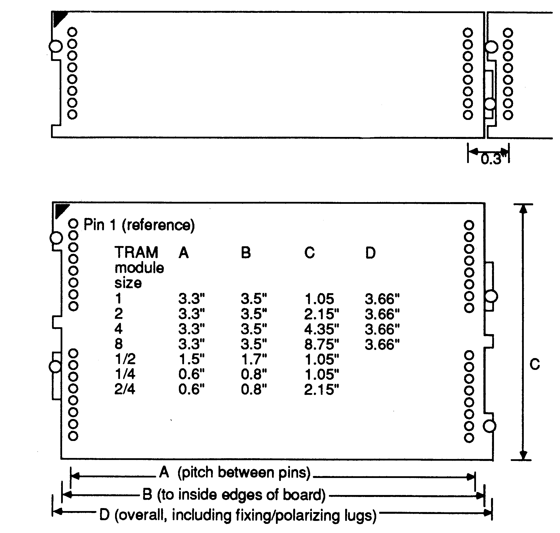
The size and spacing of module slots must conform to the mechanical specification in the Dual-In-Line Transputer Modules (TRAMs) document, the main points of which are reiterated here.
In the following, dimensions are quoted in inches for PCB length, width and related dimensions; all other dimensions are quoted in millimetres.
The basic size of a TRAM is a very wide 16 pin DIP, with 3.3” between the two rows of pins. These TRAMs fit on a 3.6” pitch on their length, and a 1.1” pitch on their width. Extra length is added beyond the pins to hold the pins, to provide for mechanical fixing, and to polarise the module shape. Modules can be made larger than the standard size by keeping the 3.3” between pins and using two or more sets of the 16 pins. They can be made smaller than the standard size, down to a 16 pin DIP with 0.6” between the two rows of pins, or 1.5” between the pins. These sizes will normally be used for single chip modules or hybrids.
The top drawing in Figure 15 shows a Size 1 module and how the jigsaw pattern fits together between adjacent modules. The lower drawing in Figure 15 shows the various sizes of TRAM. Detailed dimensions of the different sizes are given in the Dual-In-Line Transputer Modules (TRAMs) document [1].
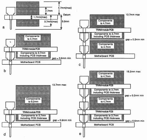
The height specifications, both above and below the TRAM PCB, are shown in Figure 16a. Figure 16b shows a module with these dimensions plugged into a motherboard.
Figure 16c shows a TRAM above components on a motherboard and the overall component height is 13.7mm, which is within normal specifications for motherboards on 0.8” centres.
It is recommended that any component reaching a maximum specified height has an insulating surface.
To provide the spacing shown in Figure 16c, the TRAM pins are implemented as a stackable socket, and an extra stackable socket is used between the motherboard socket and module pin.
Figure 16d shows an alternative component height which meets the 13.7mm overall height if the module is not above components on a motherboard. Figure 16e shows two modules stacked.
Note that the datum for component heights on both sides of the TRAM is the component side surface. This datum is also used for the stackable socket to minimize tolerance buildup.
The TRAM pins/stackable sockets defined in the Dual-In-Line Transputer Modules (TRAMs) document will plug into any standard IC socket. To meet the component heights given in Figure 16, the stackable socket must also be used on the motherboard.
Motherboard sockets for the Slot 0 SubSystem signals should be the 0.38mm or 0.4mm sockets referred to in the Dual-In-Line Transputer Modules (TRAMs) document.
Vibration tests have shown that in a normal office or laboratory environment, the TRAMs remain plugged into their sockets. In transit, however, or in an environment where there is vibration, some form of mechanical retention may be necessary.
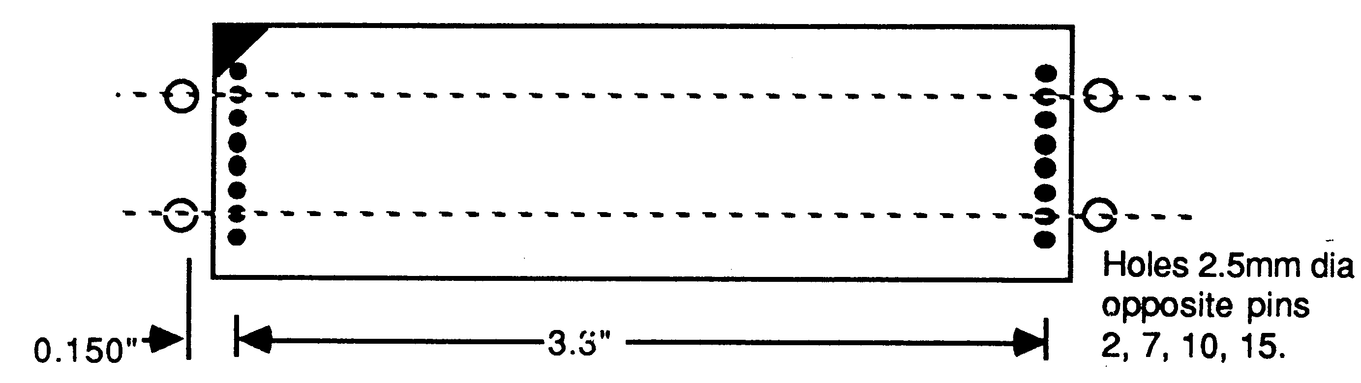
Modules have fixing holes to facilitate mechanical retention, see the Dual-In-Line TransputerModules (TRAMs) document. Similar fixing holes should be drilled in the motherboard as shown in Figure 17. M2.5 nylon bolts may be used between these fixing holes to secure the modules.
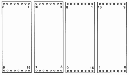
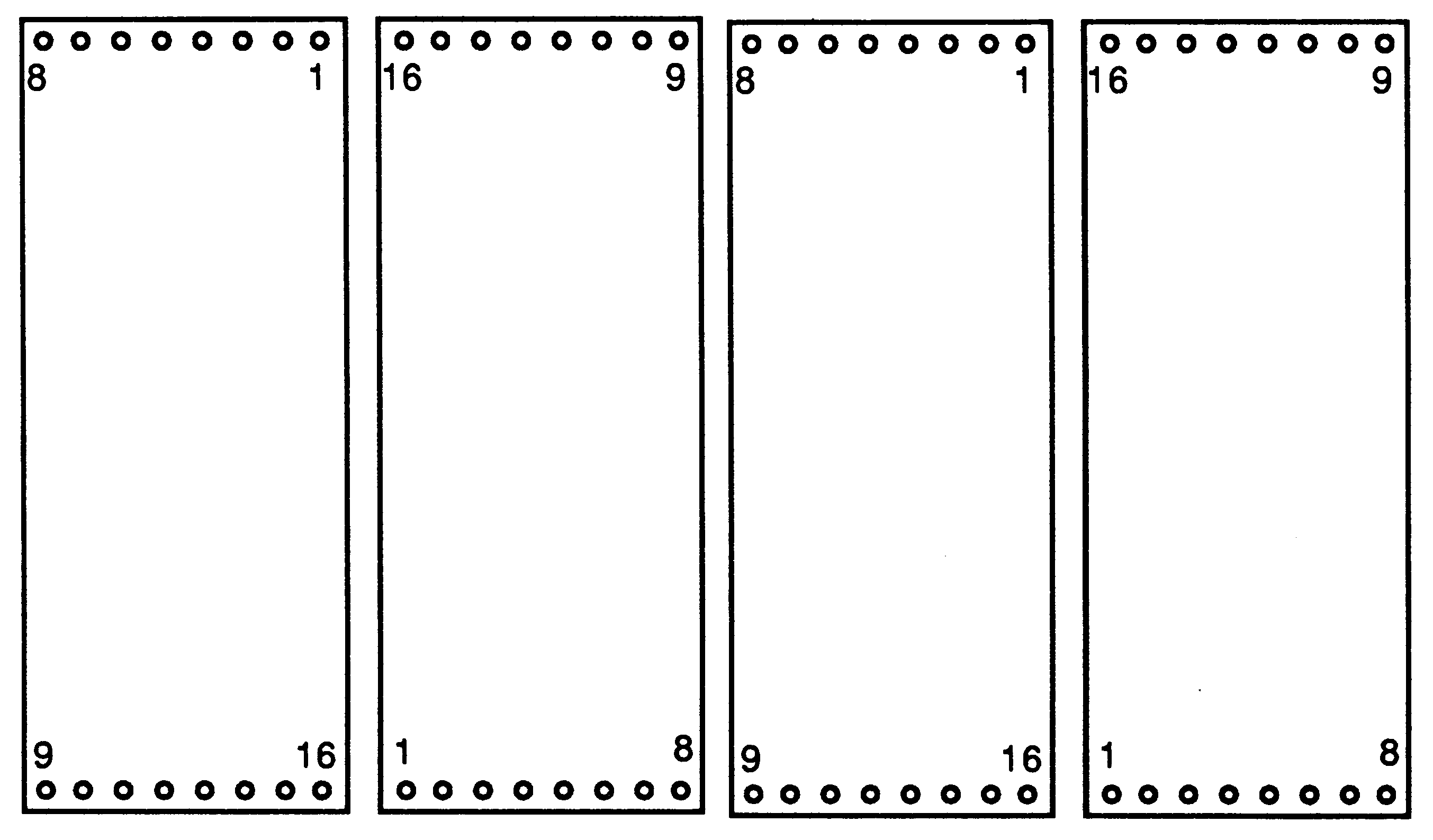
Figure 18 shows the orientation of transputer modules when mounted in slots on a motherboard. Notice how each module is rotated through 180∘ with respect to adjacent modules. This serves two purposes: cooling of Size 1 modules is improved; and it makes it possible to have Single-In-Line modules at some future date.
Connectors are necessary to enable links and system control signals to be taken from a motherboard to other boards. Several types of connector have been used on INMOS module motherboards.
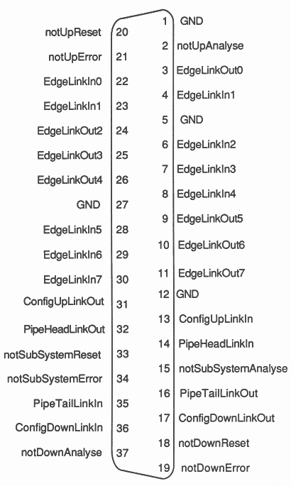
The IMS B008 module motherboard for the IBM PC uses a 37-way D-type connector, the pin-out of which is shown in Figure 19.
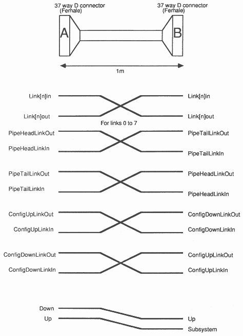
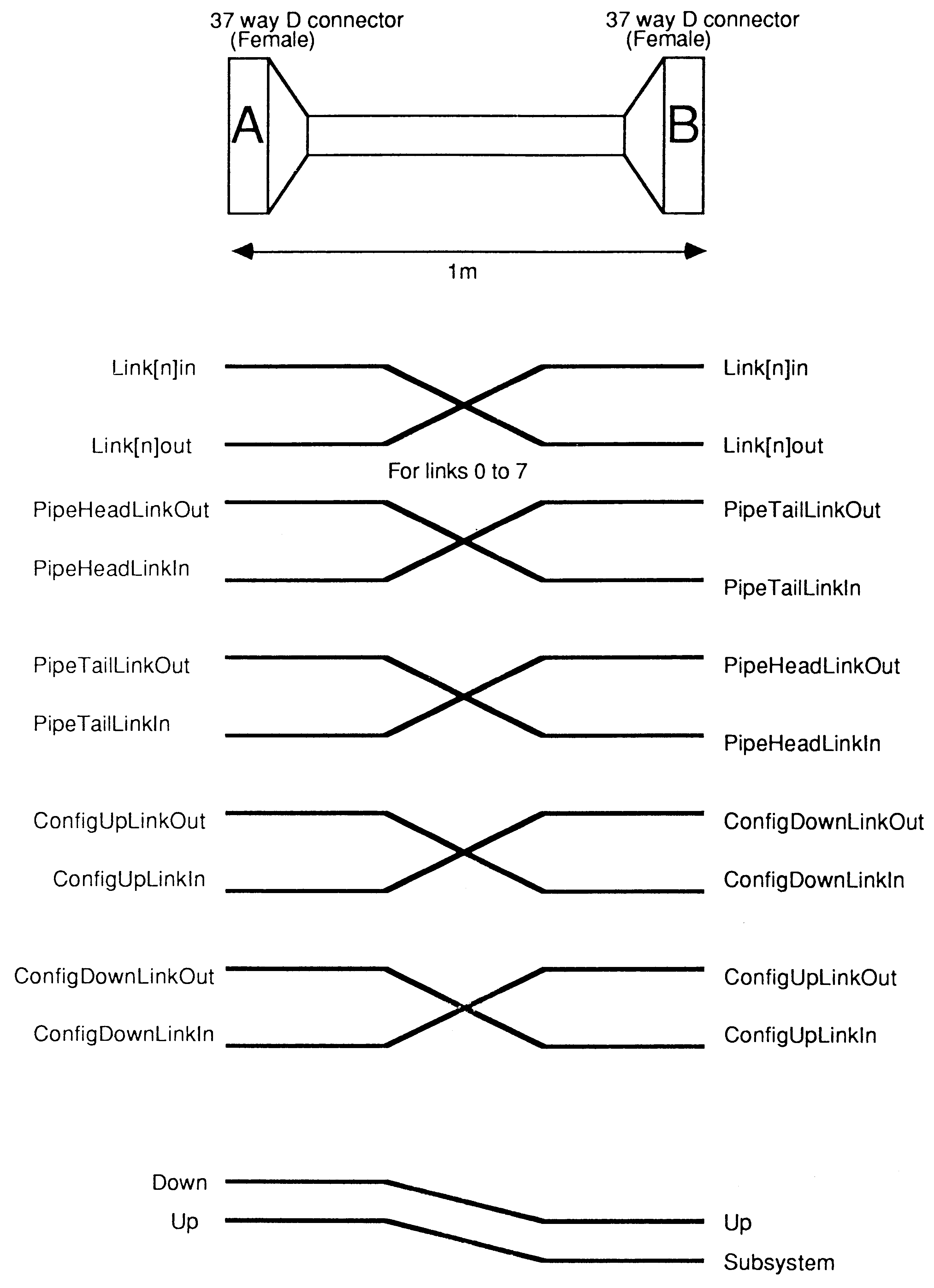
This connector provides up to twelve links (including ConfigUp, ConfigDown, PipeHead and PipeTail), plus Up, Down and Subsystem ports. A cable suitable for connecting IMS B008s together is shown diagrammatically in Figure 20.
The IMS B012 is a module motherboard in double extended Eurocard format. It has two 96-way DIN 41612 connectors. The bottom connector (P2) provides connections for eight links (including ConfigUp, ConfigDown, PipeHead and PipeTail) and Up, Down and SubSystem ports. Table 1 shows the general pinout adopted by INMOS for such a connector, making it suitable for use with module motherboards while preserving compatibility with the the rest of the INMOS range of boards. The pins marked Spare and Spare link may be used for signals and links specific to a particular application. The IMS B012 User Guide and Reference Manual describes how these pins are used on the IMS B012.
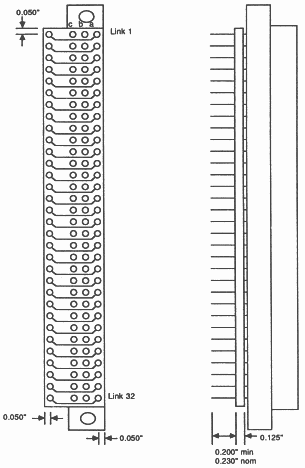
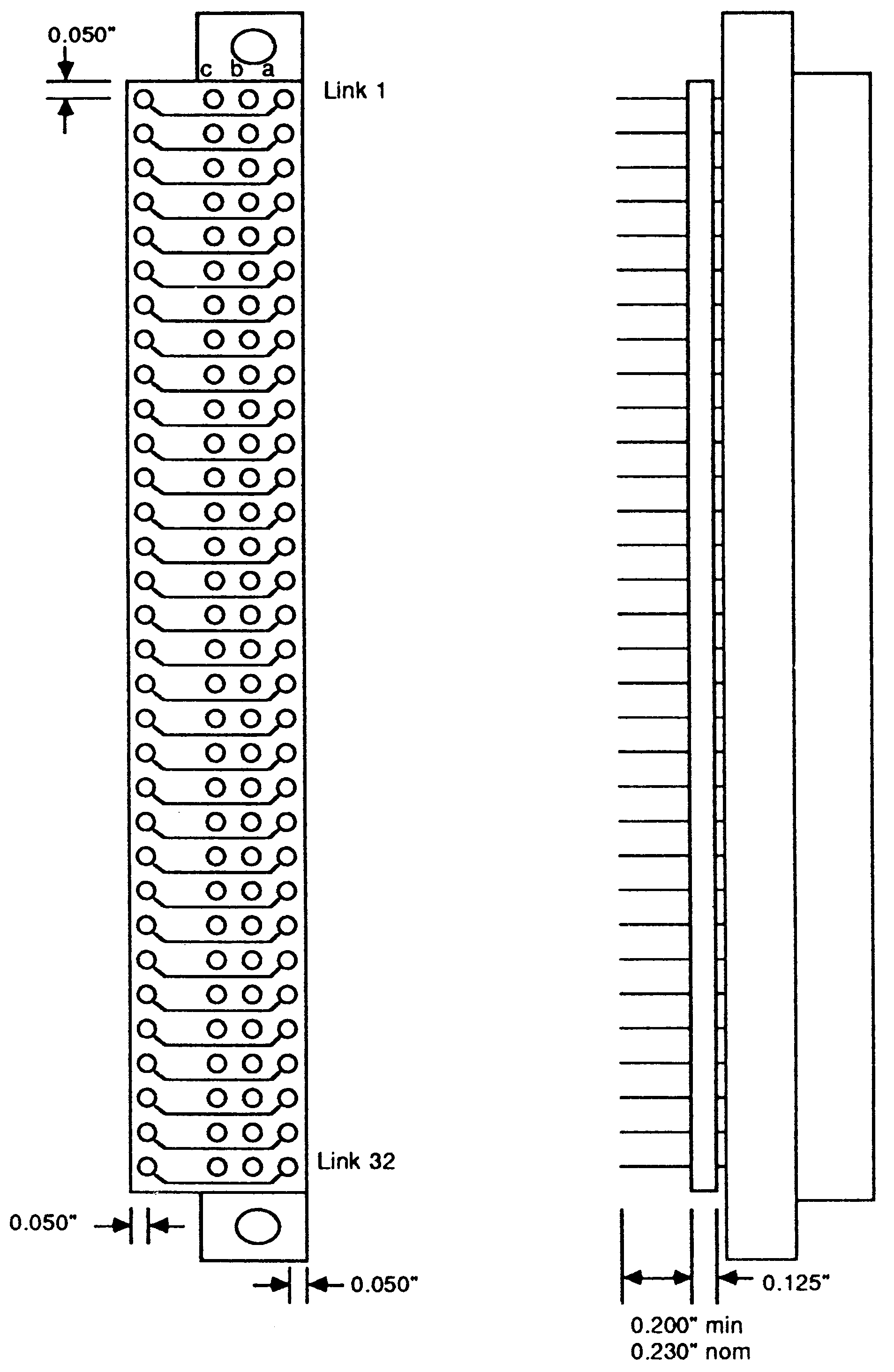
The top connector (P1) of the IMS B012 is a DIN 41612 connector that takes a special mini-backplane to provide connections to 32 links. See Figure 21 for the mechanical details and Table 2 for the pinout of this connector. On the IMS B012, the P1 connector is used to bring out links from the board’s two IMS C004s. See the IMS B012 User Guide and Reference Manual for details. The mini-backplane is available from Varelco, part number 07-8258-0940-01-00. Both the P1 and P2 connectors are used with the INMOS Link and Reset cables provided with most INMOS board products.
|
|