Gallery / Exhibition
I think, almost all people likes photos, especial people on the web. So I took some photos of my transputer stuff and created this column. Most of the pictures have a link to a high resolution image.
- Transputer die: We start with the inner values of a transputer and some basic facts.
- Transputer chips: Almost all 16 bit and 32 bit transputer family members in the ceramic PGA package.
- Transputer modules: TRAMs like IMS B411, IMS B404, IMS B427, ...
- Transputer motherboards: Carrier boards for TRAMs to be assembled in different cages. IMS B008, IMS B011, IMS B012, ...
- Evaluation boards: The first generation double extended eurocard boards (IMS B001, IMS B002, ...) and the classic IMS B004.
- Transputer cluster: Parsytec & Co.
- Associated hardware: ITEM's, VME or proprietary 19" chassis, cabinet, ...
There are no marks or copyright notice in the pictures because they are unaesthetic. However, all photographs appearing here in this gallery are the exclusive property of Michael Brüstle.
Transputer die
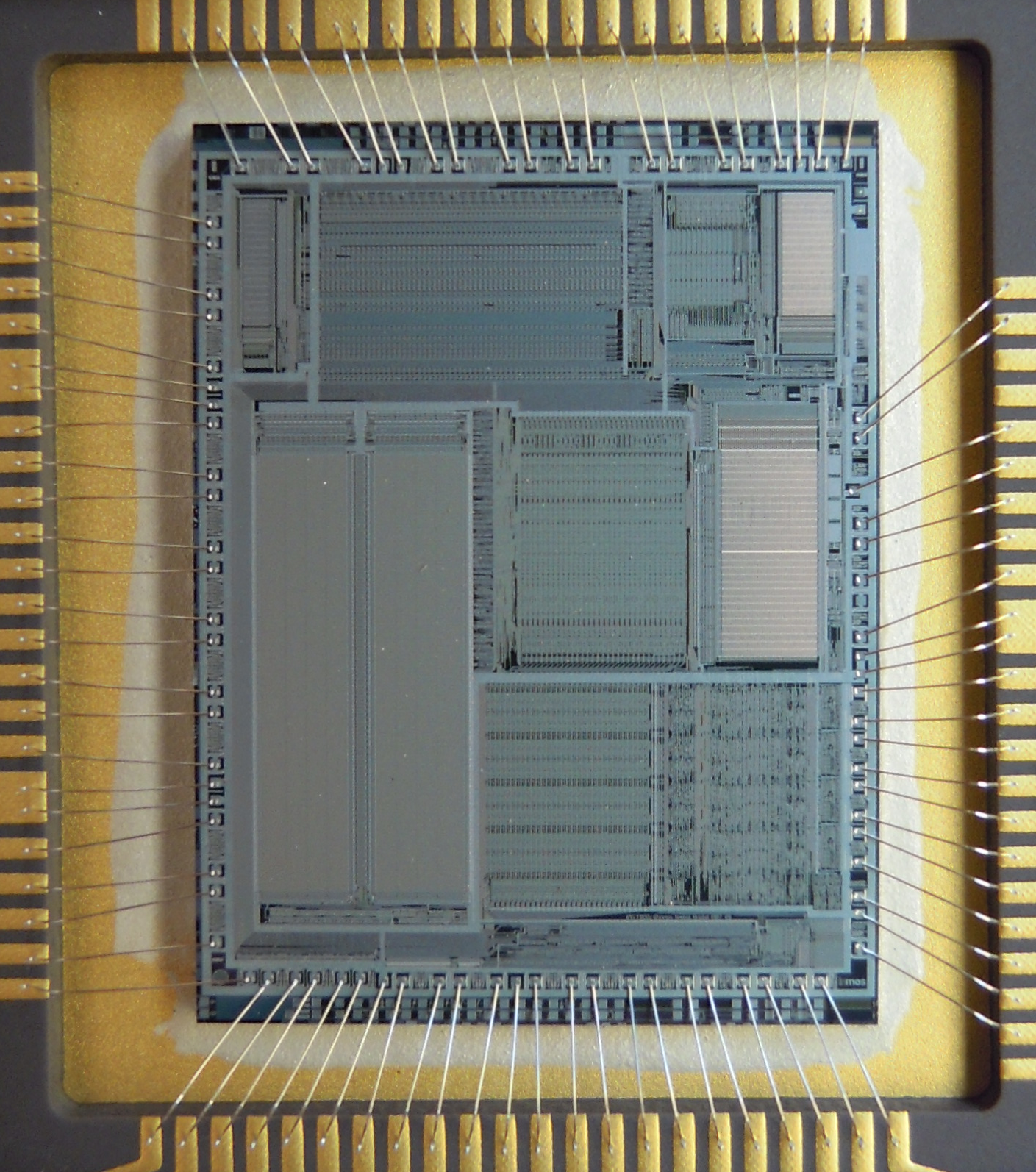
This is a die-picture of a forcible opened IMS T800C-G20S floating-point transputer.
The T800 is a 64-bit floating point member of the transputer family. He integrates a 32-bit microprocessor, a 64-bit floating point unit, four standard transputer communications links, 4 Kbytes of on-chip RAM, a memory interface and peripheral interface on a single chip.
The 64-bit floating point unit provides single length and double length operation according to the ANSI IEEE 754-1985 standard for floating point arithmetic and is able to perform floating point arithmetic operations concurrently with the processor; sustaining in excess of 1.5 Mega Flops.
The T800 uses a DMA block transfer mechanism to transfer messages between memory and other transputer products via the INMOS links. The link interfaces and the processor all operate concurrently, allowing processing to continue while data is being transferred on all of the links.
The 4 Kbytes of on chip static RAM provides a maximum data rate of 80 Mbytes/sec (20 MHz) with access for both the processor and links. The T800 can directly access a linear address space up to 4GBytes. The 32 bit wide external memory interfaces uses multiplexed data and addresses lines and provide a data rate of up to 27 Mbytes/sec.
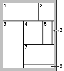
The different sections have the following functions:
1 ... 64 bit FPU mantissa with adjacent ROM
2 ... 64 bit FPU exponent with adjacent ROM
3 ... 4 Kbyte static RAM
4 ... 32 bit CPU
5 ... microcode ROM for the CPU
6 ... phase locked loop
7 ... 4 serial links
8 ... external memory interface
The gray border area is for the bonding. Pin A1 is in the upper right corner. The die is approximately 11.4mm high and 9.1mm wide. The outcome of this is a chip area of 1cm². The T800 uses 300,000 transistors on a 1.5 micron CMOS process which has one metal layer plus a low-resistance silicide interconnect layer.
About the footprint of the FPU there is also a more detailed explanation (with a block diagram) in the INMOS Technical Note "IMS T800 architecture"
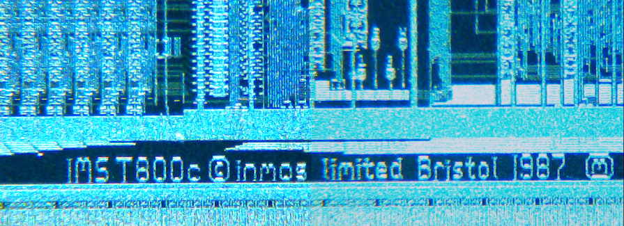
There is also a very tiny copyright note IMS T800c © inmos limited Bristol 1987 (m) between the link section and the EMI.
Transputer chips
 |
 |
 |
 |
 |
 |
 |
 |
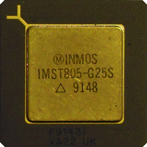 |
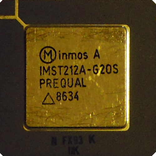
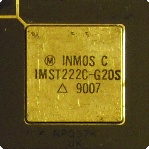
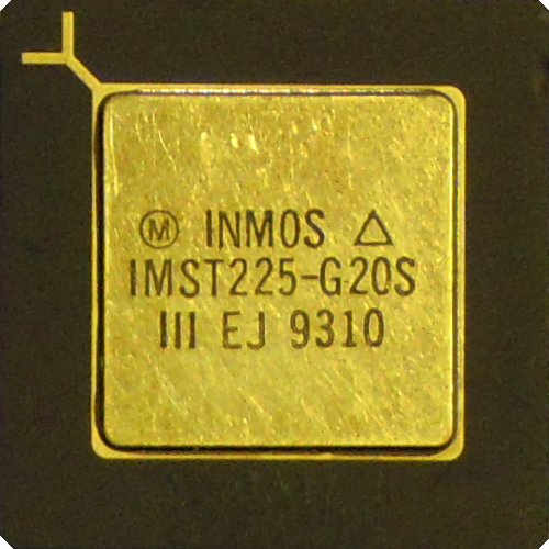
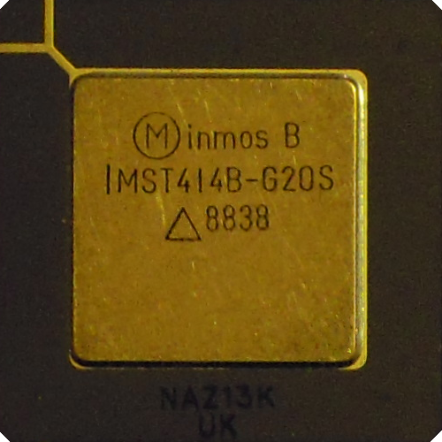
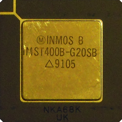
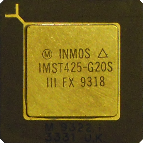
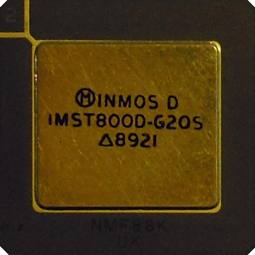
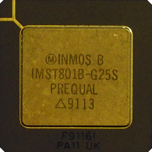
All nine different transputer types in the classic (the one and only) ceramic PGA package with the "gold" cap:
| IMS T212A | IMS T222C | IMS T225 |
| IMS T414B | IMS T400B | IMS T425 |
| IMS T800D | IMS T801 | IMS T805 |
Unfortunately the IMS M212 is missing and the IMS T426 is not available in the PGA package. I'm still searching both types for my collection.
From the other types there are many more - some with different speed grades and different revisions. My oldest transputer is a IMS T414-AG PRE QUAL 85 48.
Transputer modules
- IMS B411
- IMS B404
- IMS B427
- ...
Transputer motherboards
- IMS B008
- IMS B012
- IMS B014
- IMS B016
Evaluation boards
- IMS B001
- IMS B002
- IMS B004
Transputer cluster
- Parsytec
Associated hardware
- IMS B201 cage
- IMS B300
- VME 3 cage
- VME 5 cage